Organic light-emitting diode having a breaker construction and method for making same

A technology of light-emitting diodes and manufacturing methods, which is applied in semiconductor/solid-state device manufacturing, electrical components, electric solid-state devices, etc., can solve the problems of non-conductivity, increase the driving voltage of components, etc., and achieve the effect of best conductivity

Inactive Publication Date: 2008-05-28
AU OPTRONICS CORP
View PDF4 Cites 0 Cited by
  • Summary
  • Abstract
  • Description
  • Claims
  • Application Information

AI Technical Summary

Problems solved by technology

CuPc is an organic material and does not have conductivity, which may increase the driving voltage of the device

Method used


Image

  • Organic light-emitting diode having a breaker construction and method for making same
  • Organic light-emitting diode having a breaker construction and method for making same
  • Organic light-emitting diode having a breaker construction and method for making same

Examples


Embodiment Construction

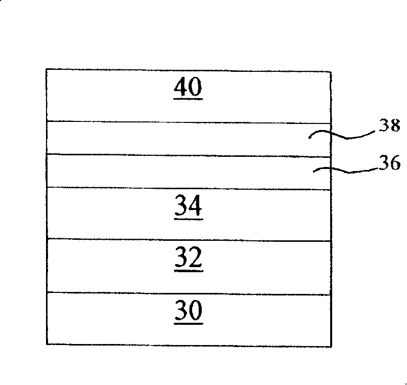
[0044] The invention is a manufacturing method of an organic light-emitting diode with a cathode buffer layer. In order to make the narration of the present invention more detailed and complete, refer to the following description and cooperate image 3 and Figure 4 schema. A detailed description of the present invention is as follows.

[0045] see image 3 , is an organic light emitting diode with a cathode buffer layer structure provided according to the first embodiment of the present invention. Firstly, an anode electrode 32 is formed on the substrate 30 . The material of the substrate 30 can be selected from transparent or opaque but reflective materials, and the anode electrode 32 can also be selected from transparent conductive materials or metal materials. The material of the above-mentioned transparent conductive electrode can be selected from materials such as indium tin oxide (Indium Tin Oxide, ITO), indium zinc oxide (Indium Zinc Oxide, IZO), and is made by sp...


PUM


Abstract

Disclosed is an organic light-emitting diode having a buffer layer structure and the method of making comprising the steps of, forming an anode electrode onto the substrate, then forming in sequence an organic luminescent layer, an electron injection cathode layer, a cathode buffer layer, finally forming a transparent cathode onto the cathode buffer layer, wherein the cathode buffer layer is made from metallic material to protect the organic luminescent layer when forming the transparent cathode.

Description

technical field [0001] The invention relates to an organic light emitting diode, in particular to an organic light emitting diode with a buffer layer structure and a manufacturing method thereof. Background technique [0002] Organic Electroluminescence Display (Organic Electroluminescence Display, OLED, OrganicEL Display) is also called Organic Light Emitting Diode (Organic Light Emitting Diode; OLED) display because of its high brightness and fast screen response. Thin and short, full-color, no viewing angle difference, no need for LCD backlight, and save light source and power consumption, so it can take the lead in replacing twisted nematic (Twist Nematic; TN) and super twisted nematic (Super Twist Nematic; STN) ) liquid crystal display market, and further replace small-size thin film transistor liquid crystal display, and become a new generation of portable information products, mobile phones, personal digital processors and portable computers commonly used display mate...

Claims


Application Information

Patent Timeline
IPC IPC(8): H01L51/40H01L51/50H01L33/00
Inventor 柯崇文
Owner AU OPTRONICS CORP
Why Eureka
Try Eureka