Semiconductor device

A semiconductor and device technology, applied in the field of semiconductor devices, can solve the problems of increased installation area, increased cost of semiconductor devices, increased cost of electronic devices, etc.

Inactive Publication Date: 2008-05-28
HITACHI LTD
View PDF4 Cites 0 Cited by
  • Summary
  • Abstract
  • Description
  • Claims
  • Application Information

AI Technical Summary

Problems solved by technology

[0004] However, in these semiconductor devices, a ground pattern is provided around each electrode, and a second ground via hole electrically connected to the ground layer is formed in the ground pattern, so the semiconductor device becomes large due to the amount of ground patterns provided.
Some problems arise when the semiconductor device becomes larger: the cost of the semiconductor device increases and the mounting area increases, thereby increasing the cost of the electronic device incorporating the semiconductor device

Method used


Image

  • Semiconductor device
  • Semiconductor device
  • Semiconductor device

Examples


Embodiment Construction

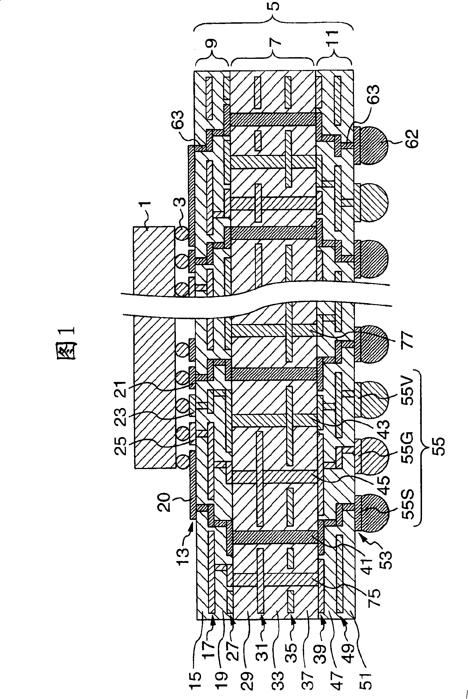
[0023] Embodiments of the present invention will be described below with reference to FIGS. 1-5.

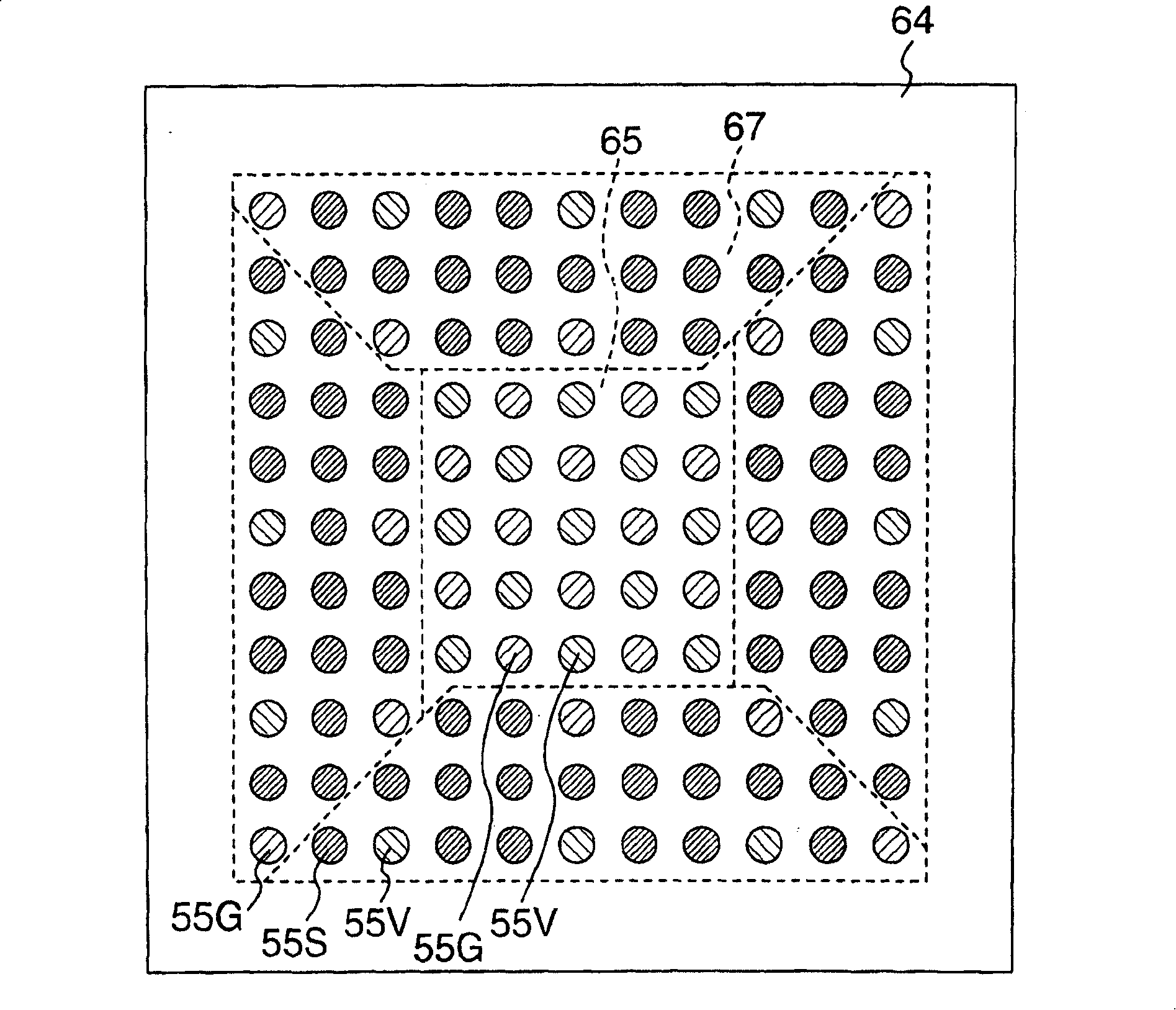
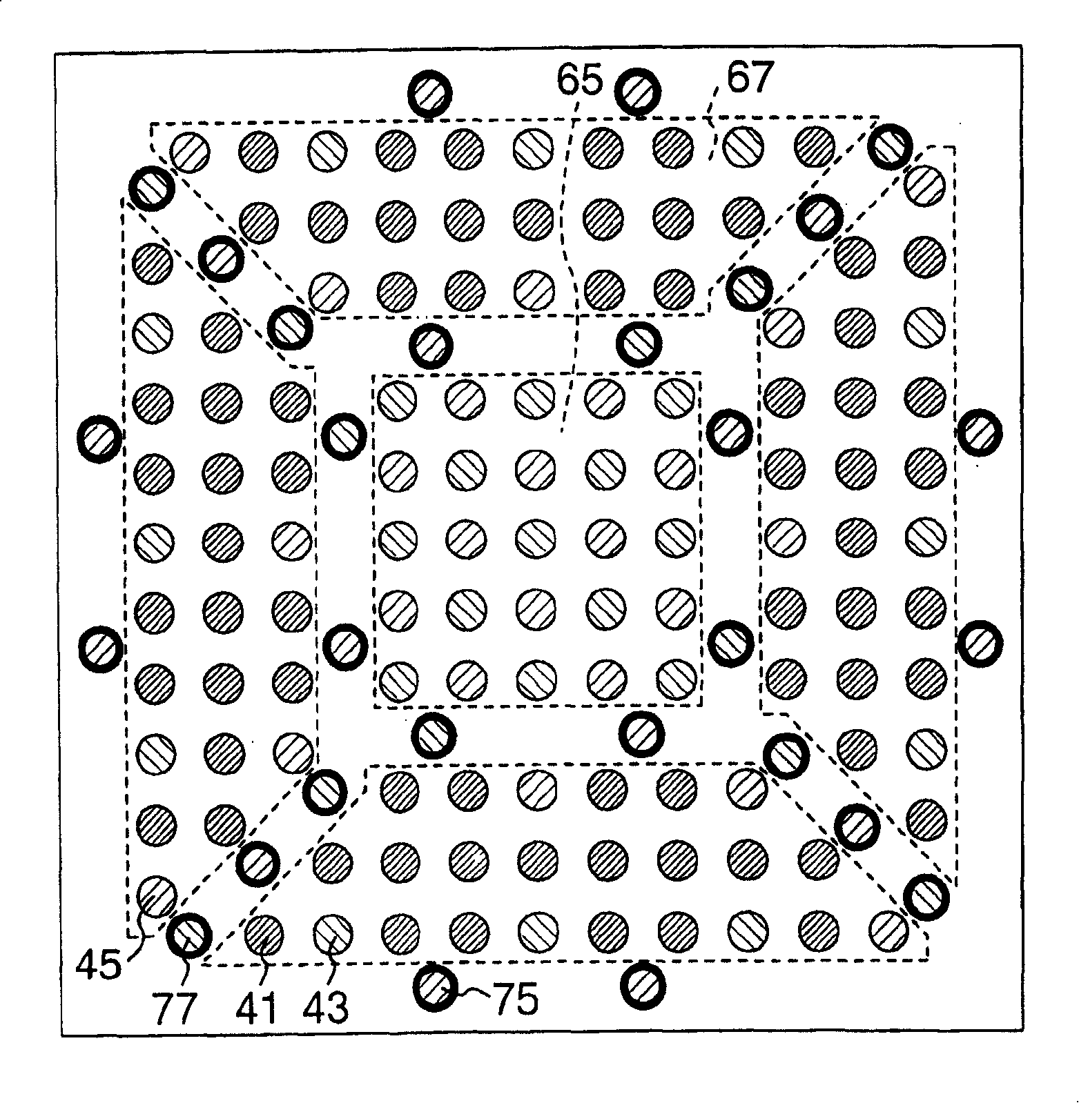
[0024] A BGA type semiconductor device according to this embodiment comprises a semiconductor chip 1 and a substrate 5 connected to the semiconductor chip 1 by connecting members such as solder balls 3, as shown in FIG. Lead terminals (not shown) of the semiconductor chip 1 are all located on the surface facing the substrate 5, and these lead terminals (not shown) are arranged in a grid form.

[0025] The substrate 5 electrically connects the grid lead ends (not shown) arranged on the semiconductor chip 1 to the main board of the electronic device, etc. to increase the interval of the lead ends, that is, its pitch. The formed core layer 7 and the surface layers 9 and 11 on both sides of the core layer 7 can form dense leads in the substrate 5 .

[0026] One of the surface layers 9 and 11 on both sides of the core layer 7 faces the semiconductor chip 1 to which the solder balls 3...


PUM


Abstract

The suppression of the scaling up of a semiconductor device and the reduction of noises. A semiconductor device comprises a base (5) provided with skin layers (9, 11) on both faces of a core layer (7) formed of a printed wiring board and a semiconductor element (1) mounted on the base (5). The semiconductor element (1) is bonded to one skin layer (9) with a bonding member (3), and external terminals (55) are arranged on the other skin layer (11). The core layer (7) has through holes (41, 43, 45, 75, 77) which electrically connect the semiconductor element (1) and the external terminals (55). The through holes (41, 43,45, 75, 77) consist of array through holes (41, 43, 45) disposed in accordance with the array of the external through holes (55) and one or more additional through holes (75, 77) provided between the array through holes (41, 43, 45).

Description

technical field [0001] The present invention relates to semiconductor devices. Background technique [0002] Ball Grid Array Semiconductor Devices (hereinafter referred to as BGA Semiconductor Devices), Grid Pin Array Semiconductor Devices (hereinafter referred to as PGA Semiconductor Devices), Land Grid Array Semiconductor Devices (hereinafter referred to as LGA Semiconductor Devices), Chip Size Packaged semiconductor devices (hereinafter referred to as CSP semiconductor devices), etc., in which the lead terminals are made in the form of a grid, because this form can increase the number of signal lines, plus other reasons, it has been widely used. [0003] In these semiconductor devices, in order to reduce electrical noise, in addition to the first ground vias electrically connected to the ground plane, it has been proposed to provide a plurality of second ground vias, which are connected to the ground plane in the ground pattern provided at the predetermined position on th...

Claims


Application Information

Patent Timeline
Patent Type & Authority Patents(China)
IPC IPC(8): H01L23/12H01L23/498H05K1/02H05K1/11H05K3/46
CPCH05K1/0216H01L2924/15311H05K3/4602H05K1/112H01L2924/01078H01L23/49827H01L2924/3011H01L23/49822H05K2201/09536H05K2201/10674H05K2201/09781H05K1/115H01L2224/16H01L2224/16225H01L23/12
Inventor 永田达也宫本诚司安藤英子
Owner HITACHI LTD
Why Eureka
Try Eureka