Semiconductor wafer package and its packaging method

A chip package, packaging method technology, applied in the direction of semiconductor devices, semiconductor/solid-state device manufacturing, semiconductor/solid-state device parts and other directions

Inactive Publication Date: 2007-11-21
沈育浓
View PDF5 Cites 0 Cited by
  • Summary
  • Abstract
  • Description
  • Claims
  • Application Information

AI Technical Summary

Problems solved by technology

However, the method disclosed in the above-mentioned U.S. patent needs to use a substrate to mount the semiconductor chip. Therefore, different semiconductor chips require different substrates in terms of size or function. Therefore, in terms of cost and There is a need for improvement in the packaging procedure

Method used


Image

  • Semiconductor wafer package and its packaging method
  • Semiconductor wafer package and its packaging method
  • Semiconductor wafer package and its packaging method

Examples


Embodiment Construction

[0148] Before the present invention is described in detail, it should be noted that throughout the description, the same elements are designated by the same reference numerals.

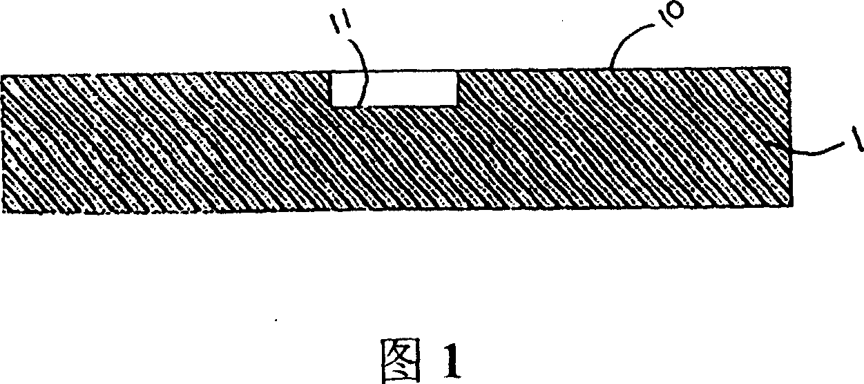
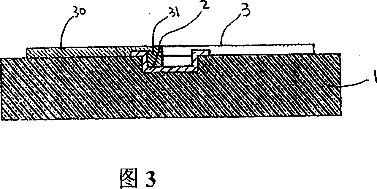
[0149] 1 to 10 show the first preferred embodiment of the packaging method of the semiconductor chip package of the present invention.

[0150] Referring to FIG. 1 in conjunction with FIG. 45, a semiconductor wafer 1 is first provided. The semiconductor wafer 1 has a bonding pad mounting surface 10 and a plurality of bonding pads 11 mounted on the bonding pad mounting surface 10 (in the drawings, only one bonding pad 11 is shown).

[0151] It should be noted that the semiconductor wafer 1 shown in FIG. 1 may be a single wafer that has been diced from the wafer, but may also be a wafer that has not been diced from the wafer.

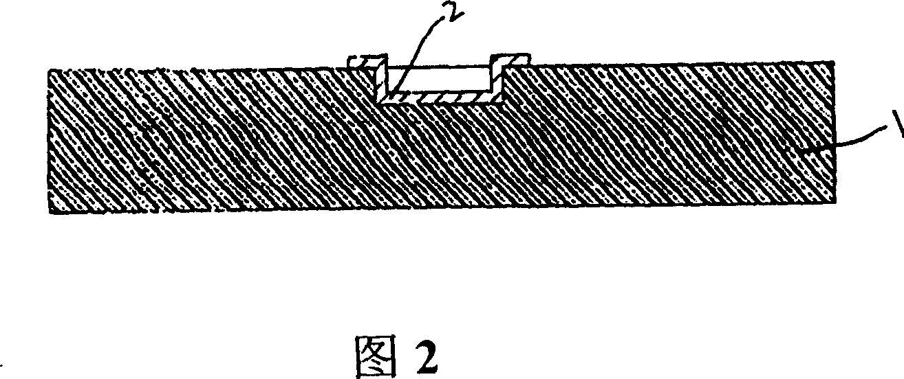
[0152] Next, as shown in FIG. 2 , a plating layer 2 is formed on each pad 11 of the chip 1 . The plating layer 2 will extend slightly onto the pad mounting surface 10 of the wa...


PUM


Abstract

The invention discloses a semiconductor wafer packager and its packaging method, and the packager comprises: a semiconductor wafer with a pad installation surface and several pads installed on the pad installation surface; several conductors, each provided with an extension part and a conductive connection part; a protective layer, able to cover these conductors, formed on the pad installation surface and formed with several through holes connected to the corresponding conductors; and several conductive balls, each formed in the corresponding through hole and connected with the corresponding conductor. The invention has the advantages of simplifying packaging procedure, small packager bulk, low packaging cost, etc.

Description

[Technical field] [0001] The present invention relates to a semiconductor chip package and a packaging method thereof. [Background technique] [0002] In the early days, most of the packaging methods of semiconductor chips used lead frames as a medium for the electrical connection between the internal circuit of the chip and the external circuit. However, the integrated circuit packaged in this way is larger in size and the transmission speed of the signal is slower. Later, the ball grid array (BGA) packaging method appeared. As disclosed in US Patent No. 5,384,689. The integrated circuit packaged by the BGA packaging method is smaller in size, and the signal transmission speed will be faster. However, the method disclosed in the above-mentioned US patent requires the use of a substrate to mount the semiconductor wafer. Therefore, semiconductor wafers with different sizes or functions require different substrates. Therefore, the cost and There is a need for improvement i...

Claims


Application Information

Patent Timeline
Patent Type & Authority Patents(China)
IPC IPC(8): H01L23/48H01L23/29H01L23/12H01L21/50
CPCH01L2224/13
Inventor 沈育浓
Owner 沈育浓
Why Eureka
Try Eureka