Semiconductor integrated circuit arrangement fabrication method
a technology of integrated circuit and fabrication method, which is applied in the direction of electrical equipment, decorative surface effects, decorative arts, etc., can solve the problems of large increase in the cost of the etching system, inability to obtain electrons with uniform energy necessary for realizing the control in plasma, and difficulty in achieving the control by a conventional etching method. , to achieve the effect of maximizing the selection ratio
- Summary
- Abstract
- Description
- Claims
- Application Information
AI Technical Summary
Benefits of technology
Problems solved by technology
Method used
Image

Examples
embodiment 1
[0075][Embodiment 1]
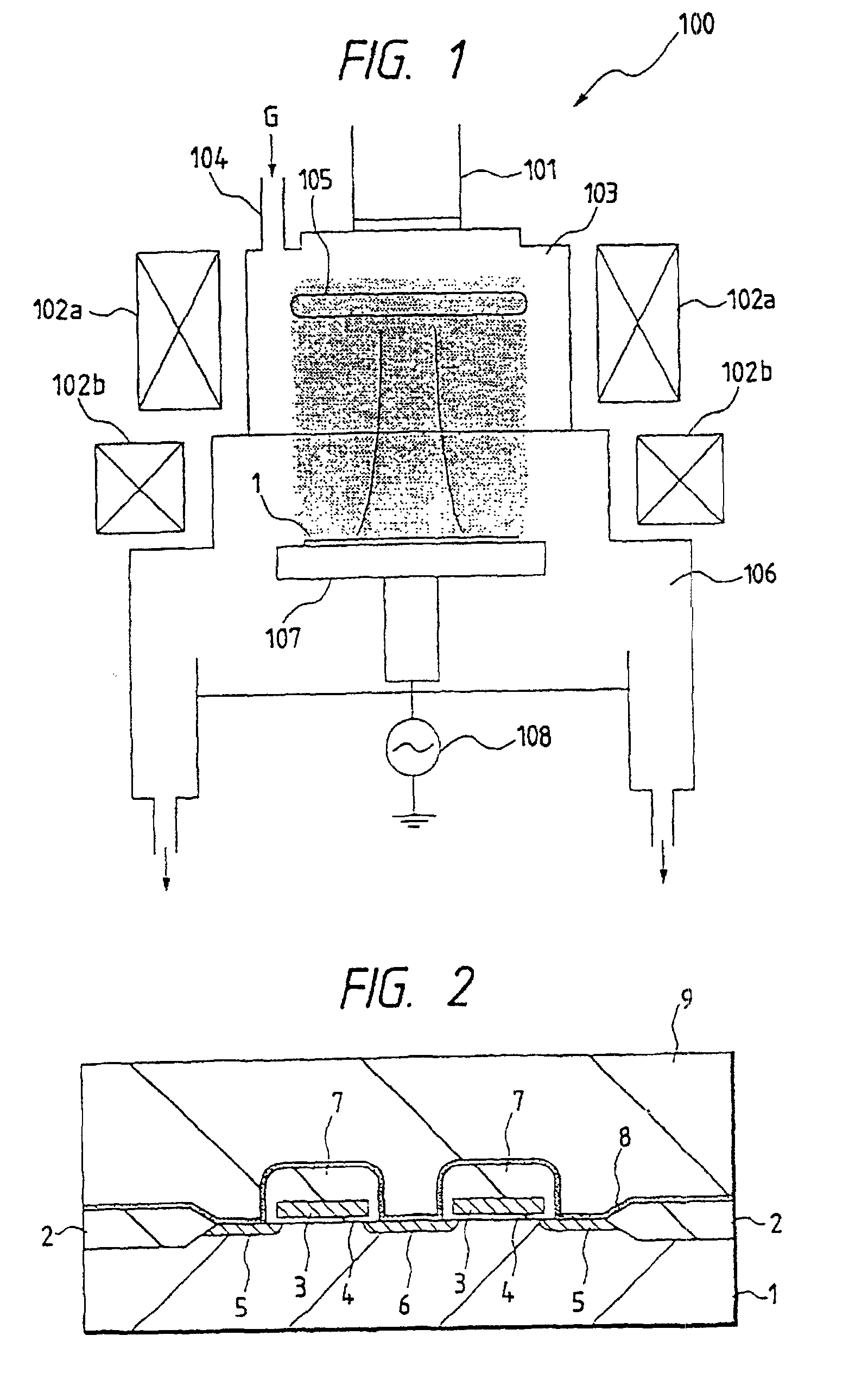
[0076]FIG. 1 is a schematic view of a microwave plasma etching system 100 used in this embodiment. The system 100 includes a microwave guide 101, magnets 102a and 102b, a plasma generation change 103, and a a reaction chamber 106. Microwaves of 2.45 GHz generated by a magnetron are introduced into the plasma generation chamber 103 through the microwave guide 101. Moreover, a material gas G is introduced into the plasma generation chamber 103 through a gas introduction port 104.
[0077]By introducing microwaves into the plasma generation chamber 103 and generation a magnetic field of approx. 1 KG by the magnets 102a and 102b, the material gas G is transformed into a plasma by electron cyclotron resonance at an ECR position 105 with a flux density of approx. 875 G.
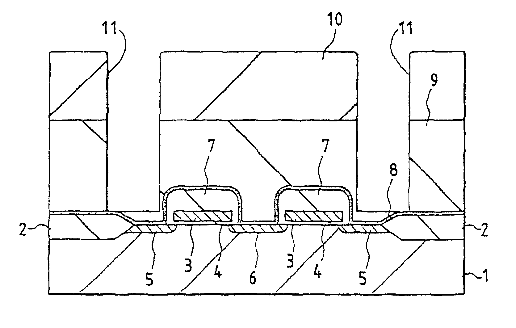
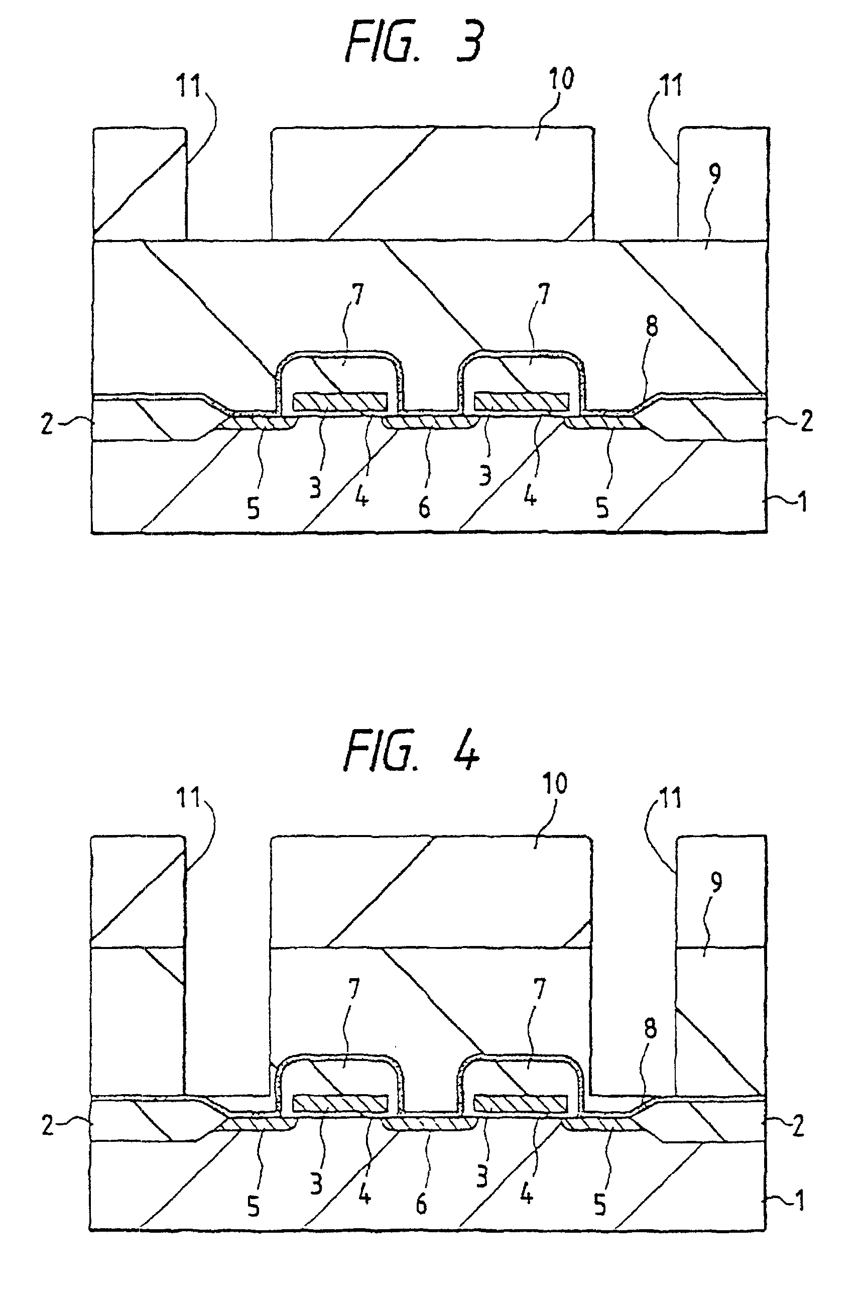
[0078]In this case, neutral dissociated species and ionic dissociated species generated from the material gas G are transferred to the surface of a semiconductor substrate (wafer) 1 in the reaction chamber ...
embodiment 2
[0094][Embodiment 2]
[0095]FIG. 7 is a schematic view of a plasma etching system 200 used in this embodiment. The plasma etching system 200 is provided with an antenna 202 around a quartz cylinder 201 so as to introduce electromagnetic waves into the cylinder 201 by applying a radio frequency to the antenna 202. Double coils 204 and 205 are provided to the outside of a vacuum chamber 203 so as to generate a magnetic field in the axial direction. A material gas G introduced through a gas introduction port 206 is transformed into a plasma by the axis-directional magnetic field and the radio frequency, and neutral dissociated species and ionic species generated during this time are transferred to the surface of the semiconductor substrate 1 where etching is performed.
[0096]Embodiment 1 uses the photoresist pattern 10 as a mask for etching the BPSG film 9. In this case, however, the products produced when photoresist is etched have an influence on the selectivity that must be considered....
embodiment 3
[0107][Embodiment 3]
[0108]FIG. 13 is a schematic view of a microwave plasma etching system 300 used in this embodiment. The system 300 includes a microwave guide 301, a magnet 302, and a plasma generation chamber303. Microwaves of 24.5 GHz generated by a magnetron are introduced into the plasma generation chamber 303 through the microwave guide 301.
[0109]A plasma of an inert gas introduced through a gas introduction port 304 is generated in the plasma generation chamber 303.
[0110]A plurality of grid electrodes 306 are provided along the boundary between the plasma generation chamber 303 and a reaction chamber 305 and only ions (i.e., not electrons) the plasma are introduced into the reaction chamber 305 by alternately changing the potentials of the grid electrodes 306 to positive and negative states. Metastable atoms of the inert gas is introduced into the reaction chamber 305 while diffusing isotropically because they are not influenced by an electric field.
[0111]A reaction gas is ...
PUM
| Property | Measurement | Unit |
|---|---|---|
| Fraction | aaaaa | aaaaa |
| Fraction | aaaaa | aaaaa |
| Length | aaaaa | aaaaa |
Abstract
Description
Claims
Application Information
 - R&D
- Intellectual Property
- Life Sciences
- Materials
- Tech Scout
- Unparalleled Data Quality
- Higher Quality Content
- 60% Fewer Hallucinations
Browse by: Latest US Patents, China's latest patents, Technical Efficacy Thesaurus, Application Domain, Technology Topic, Popular Technical Reports.
© 2025 PatSnap. All rights reserved.Legal|Privacy policy|Modern Slavery Act Transparency Statement|Sitemap|About US| Contact US: help@patsnap.com