Method for forming contact hole in semiconductor device

a contact hole and semiconductor technology, applied in semiconductor/solid-state device manufacturing, basic electric elements, electric devices, etc., can solve the problems of reducing the etching efficiency of the etching process, and producing the above described problems. , to achieve the effect of maximizing the selective ratio of the oxide layer, high resolution and simplifying the process

Inactive Publication Date: 2006-01-05
SK HYNIX INC
View PDF5 Cites 15 Cited by
  • Summary
  • Abstract
  • Description
  • Claims
  • Application Information

AI Technical Summary

Benefits of technology

[0033] It is, therefore, an object of the present invention to provide a method for forming a plurality of contact holes in a semiconductor device capable of maximizing a selective ratio of an oxide layer used as an inter-layer insulation layer during an etching process requiring a high resolution and simplifying a process.

Problems solved by technology

Furthermore, as pitch decreases and a vertical thickness of the pitch increases, there is a lack of an etch margin during performing an etching process, i.e., an etching process for forming a contact between gate electrode patterns.
The pattern deformation at the fluoride based gas is happened because of a decrease in a depositing thickness of a photoresist caused by a shortness of a wavelength of the light source used for forming the fine pattern along with a structural problem of the photoresist used for the photolithography process using ArF or F2 light source.
Accordingly, when using the photoresist for ArF and F2 that are photo-exposure materials of a next generation for the photolithography process, the photoresist pattern deformation becomes serious during the SAC etching process.
Meanwhile, in case of applying the photolithography process of a high resolution using ArF or F2 light source to the SAC etching process, the above described problems are produced.
However, when using the above described hard mask material, there is a disadvantage of certainly removing the hard mask after forming the contact hole in order to form a plug applying a selective epitaxial growth method used for a device requiring much higher conductivity.
Furthermore, in case of etching the oxide layer which is a main material to form the inter-layer insulation layer, a selective ratio between the photoresist and the oxide layer or in case of using the polysilicon layer, the tungsten layer or the nitride layer as the hard mask, the selective ratio between the polysilicon layer, the tungsten layer or the nitride layer and the oxide layer can hardly meet a selective ratio, i.e., a selective ratio required at a design rule with a size equal to or less than approximately 100 nm and with a size equal to or less than approximately 80 nm, equal to or greater than several tens to one to the fluoride gas.

Method used


Image

  • Method for forming contact hole in semiconductor device
  • Method for forming contact hole in semiconductor device
  • Method for forming contact hole in semiconductor device

Examples


Embodiment Construction

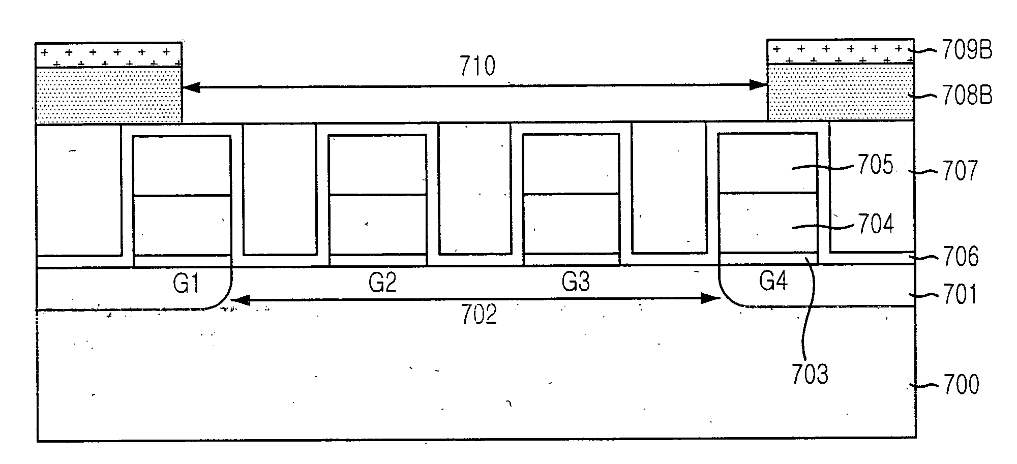
[0045] Hereinafter, a method for forming a plurality of contact holes in a semiconductor device in accordance with a preferred embodiment of the present invention will be explained in detail with reference to the accompanying drawings.

[0046]FIG. 6 is a flow chart illustrating a SAC etching process in accordance with the present invention. With reference to FIG. 6, the SAC etching process in accordance with the present invention will be explained.

[0047] First, a conductive pattern such as a gate electrode is formed and an etch stop layer is formed thereon at step S601. Subsequently, an inter-layer insulation layer is formed on a substrate provided with the conductive pattern and the etch stop layer at step S602. The inter-layer insulation layer is formed by using a typical oxide layer based material and the etch stop layer is formed by using a nitride layer based material having both insulation and a selective ratio to the oxide layer.

[0048] Subsequently, an upper portion of the i...


PUM


Abstract

Disclosed is a method for forming a plurality of contact holes in a semiconductor device. The method includes the steps of: forming an oxide-based layer on a substrate; forming an organic polymer layer on the oxide-based layer; forming a photoresist pattern on the organic polymer layer to form the plurality of contact holes; etching the organic polymer layer by using the photoresist pattern as an etch mask, thereby forming a hard mask; etching the oxide-based layer by using the photoresist pattern and the hard mask as an etch mask; and removing the photoresist pattern and the hard mask by performing a photoresist strip process, thereby obtaining the plurality of contact holes.

Description

FIELD OF THE INVENTION [0001] The present invention relates to a method for fabricating a semiconductor device; and more particularly, to a method for forming a plurality of contact holes in a semiconductor device by using a self align contact (SAC) etching process. DESCRIPTION OF RELATED ARTS [0002] A vertical arrangement structure of a unit device is used as integration of a semiconductor device increases, and a pad or a plug forming technology is used for electrical interconnection of the unit devices. At present, this contact pad forming technology is widely used as for a semiconductor device process technology. [0003] Furthermore, as pitch decreases and a vertical thickness of the pitch increases, there is a lack of an etch margin during performing an etching process, i.e., an etching process for forming a contact between gate electrode patterns. Accordingly, a self align contact (SAC) etching process is introduced to improve an etch selectivity and obtain an etch profile, and ...

Claims


Application Information

Patent Timeline
Patent Type & Authority Applications(United States)
IPC IPC(8): H01L21/469
CPCH01L21/76897H01L21/31144H01L21/28
Inventor LEE, MIN-SUKLEE, SUNG-KWONLEE, DONG-DUK
Owner SK HYNIX INC
Why Eureka
Try Eureka