Charged particle beam device
a charge-pulverized particle and beam technology, applied in the direction of electric discharge tubes, basic electric elements, electrical apparatus, etc., can solve the problem of difficult control of the orbit of secondary electrons independently, and achieve the effect of suppressing high-order off-axis chromatic aberration and high-efficiency detection
- Summary
- Abstract
- Description
- Claims
- Application Information
AI Technical Summary
Benefits of technology
Problems solved by technology
Method used
Image
Examples
first embodiment
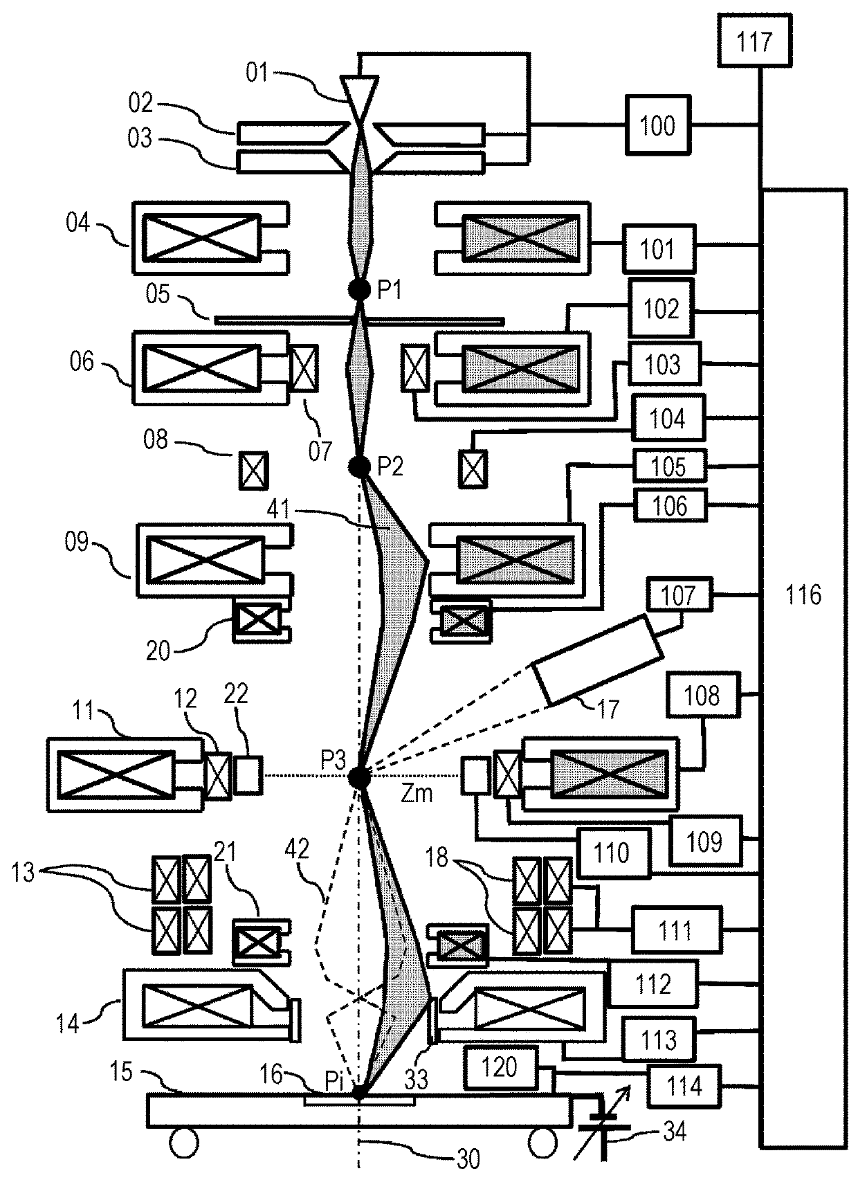
[0030]FIG. 1 is a schematic diagram of an optical configuration according to a first embodiment. In the first embodiment, the case in which a deflector and a lens are used to generate aberration necessary for aberration correction of a primary electron at the time of beam inclination will be described.
[0031]First, the case in which the primary electron is vertically incident on a sample and a focusing position of a secondary electron is not controlled will be described. A voltage is applied between a cathode 01 and a first anode 02 by an electron gun control unit 100 and a primary electron 41 is emitted at a predetermined current density. An acceleration voltage is applied between the cathode 01 and a second anode 03 by the electron gun control unit 100 and the primary electron 41 is accelerated and is ejected to a rear step. After the primary electron 41 is focused on a point P1 on an optical axis 30 by a first condenser lens 04 controlled by a first condenser lens control unit 101...
second embodiment
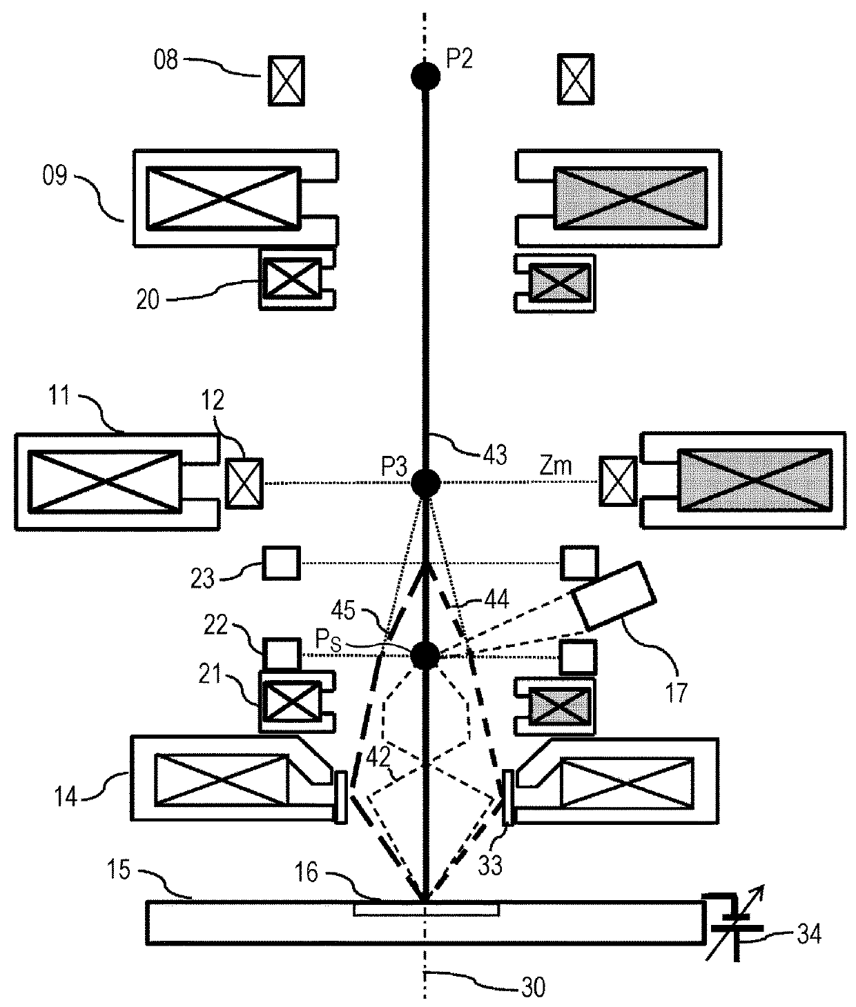
[0066]In this embodiment, a preferable configuration is provided with respect to the case in which a secondary electron deflection EXB 22 cannot be disposed on an object plane Zm of an objective lens 14, from design limitations in the first embodiment. FIG. 2 is an outline diagram of a configuration of an optical system according to this embodiment. In this embodiment, the secondary electron deflection EXB 22 is disposed between a high-order off-axis chromatic aberration suppression lens 11 and a secondary electron focusing lens 21 disposed on the object plane Zm of the objective lens 14. In addition, a dispersion adjustment EXB 23 is disposed newly between the secondary electron deflection EXB 22 and the high-order off-axis chromatic aberration suppression lens 11. A deflector 17 is disposed between the dispersion adjustment EXB 23 and the secondary electron deflection EXB 22.
[0067]In this embodiment, the strengths of the objective lens 14 and the secondary electron focusing lens 2...
third embodiment
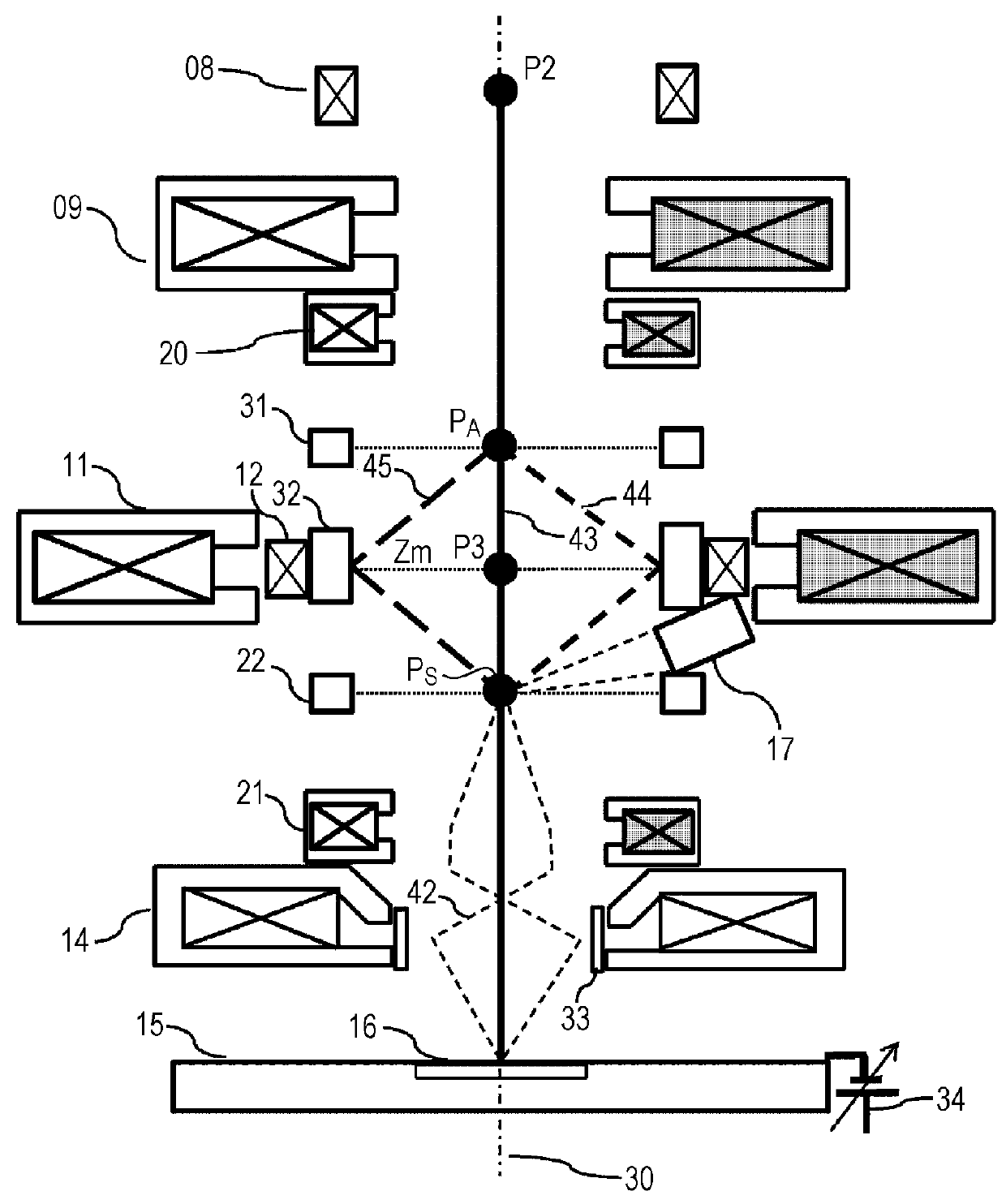
[0070]In this embodiment, a preferable configuration in which high-order off-axis chromatic aberration is not generated is provided with respect to the case in which chromatic dispersion applied from a secondary electron deflection EXB 22 to a primary electron causes high-order off-axis chromatic aberration at the time of beam inclination to become notable, when each of an inclination angle and a secondary electron deflection angle is a large angle equal to or higher than 10°, in the first embodiment.
[0071]FIG. 3 is a schematic diagram of a configuration according to this embodiment. In this embodiment, the secondary electron deflection EXB 22 is disposed between a high-order off-axis chromatic aberration suppression lens 11 and a secondary electron focusing lens 21 disposed on an object plane Zm of an objective lens 14. A detector 17 is disposed between the high-order off-axis chromatic aberration suppression lens 11 and the secondary electron deflection EXB 22. In addition, a seco...
PUM
 Abstract
Description
Claims
Application Information
 - R&D
- Intellectual Property
- Life Sciences
- Materials
- Tech Scout
- Unparalleled Data Quality
- Higher Quality Content
- 60% Fewer Hallucinations
Browse by: Latest US Patents, China's latest patents, Technical Efficacy Thesaurus, Application Domain, Technology Topic, Popular Technical Reports.
© 2025 PatSnap. All rights reserved.Legal|Privacy policy|Modern Slavery Act Transparency Statement|Sitemap|About US| Contact US: help@patsnap.com


