
Solar cell manufacturing method

a manufacturing method and solar cell technology, applied in the field of solar cell manufacturing methods, can solve the problems of reducing the lifetime of minority carriers, remarkably lower conversion efficiency of thinner silicon substrates, etc., and achieves the effects of reducing manufacturing costs, improving production efficiency, and being easy to handl

Active Publication Date: 2018-04-24
TOSHIBA MITSUBISHI-ELECTRIC IND SYST CORP +2
View PDF13 Cites 0 Cited by
  • Summary
  • Abstract
  • Description
  • Claims
  • Application Information

AI Technical Summary

Benefits of technology

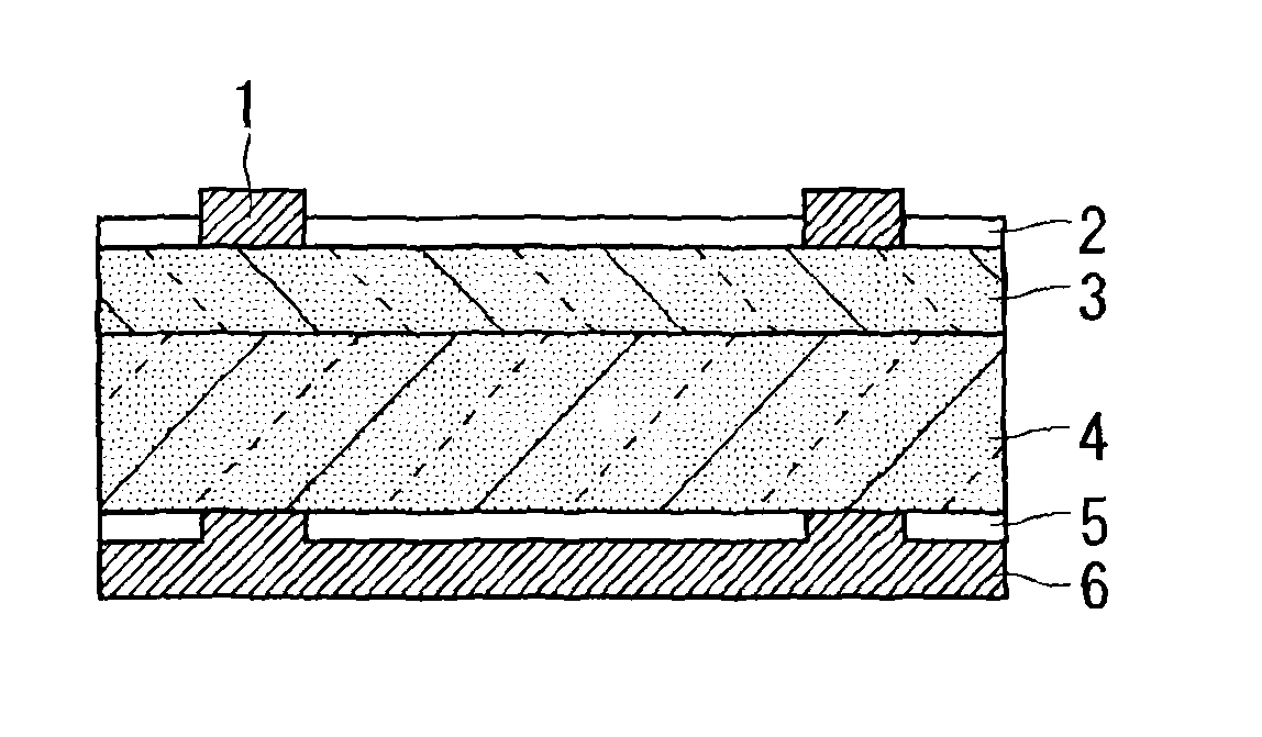
[0011]The method for manufacturing solar cell according to the present invention includes the steps (A) preparing the silicon substrate of p-type conductivity, (B) forming the passivation film on the main surface of the silicon substrate, and (C) producing the solar cell using the silicon substrate including the passivation film formed thereon. The step (B) includes the steps of (B-1) misting the solution containing aluminum elements and (B-2) spraying the misted solution onto the main surface of the silicon substrate in the atmosphere to form the passivation film being an aluminum oxide film.
[0012]This allows for the formation of a back surface passivation film made of the aluminum oxide film on the p-type silicon substrate through the use of a material that is inexpensive and easy to handle. The method eliminates the need for, for example, a vacuum processing, thus enabling the reduction of manufacturing cost. The film forming processing does not inflict damage to the p-type silicon substrate. The method also achieves the improvement of production efficiency.

Problems solved by technology

Unfortunately, thinner silicon substrates have remarkably lower conversion efficiency.
This is because, for example, a large number of defects in the front surface of the silicon substrate having a conductivity mainly cause the reduction in the lifetime of minority carriers (for example, electrons in a p-type substrate) generated by irradiation with light.

Method used


Image

  • Solar cell manufacturing method
  • Solar cell manufacturing method

Examples


embodiment 1

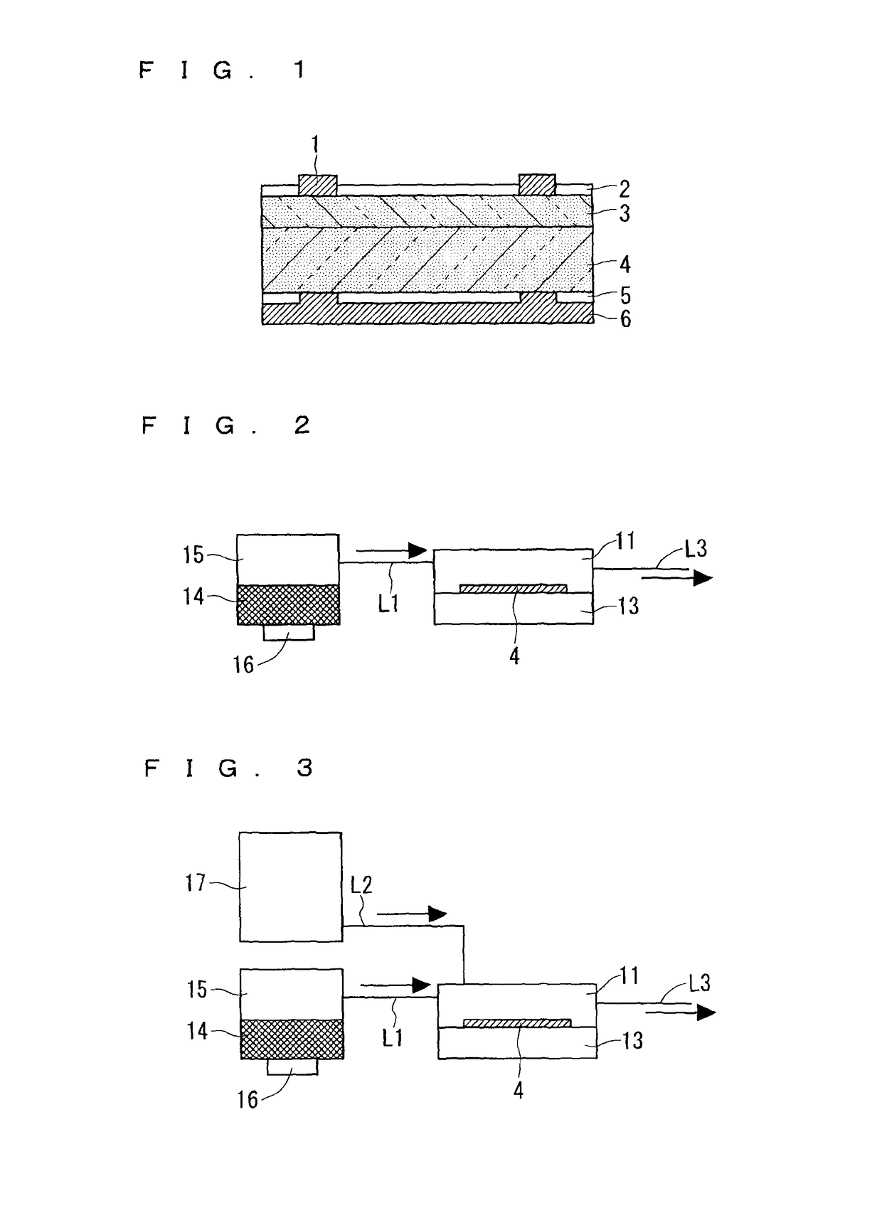
[0023]FIG. 2 is a view of a schematic configuration of a film forming apparatus capable of implementing the method for forming the aluminum oxide film 5 according to the present embodiment.

[0024]As shown in FIG. 2, the film forming apparatus includes a reactor 11, a heater 13, a solution container 15, and a mist forming apparatus 16.

[0025]In the film forming apparatus, a given solution 14 that has been misted is sprayed onto the back surface of the p-type silicon substrate 4, whereby the aluminum oxide film 5 is formed on the back surface of the p-type silicon substrate 4.

[0026]While the p-type silicon substrate 4 is placed on the heater 13, mist (the aqueous solution 14 having a small particle diameter) is supplied into the reactor 11 in the atmosphere, and then, the aluminum oxide film 5 is formed on the back surface of the p-type silicon substrate 4 as a result of a given reaction. Note that the front surface of the p-type silicon substrate 4 is placed on the heater 13.

[0027]The ...

embodiment 2

[0041]The inventors vigorously performed a number of different experiments, analyses, and the like, thus successfully finding the method for forming the aluminum oxide film 5 that significantly improves the lifetime of carriers. That is, the inventors have successfully found film forming conditions for increasing the passivation effects of the aluminum oxide film 5. The following describes the film forming method.

[0042]FIG. 3 is a view of a schematic configuration of a film forming apparatus capable of implementing the method for forming the aluminum oxide film 5 according to the present embodiment.

[0043]As is clear from the comparison between FIG. 2 and FIG. 3, the film forming apparatus according to the present embodiment has the configuration in FIG. 2 and additionally includes an ozone generator 17. The following describes the part distinct from the configuration in FIG. 2.

[0044]The ozone generator 17 is capable of generating ozone. For example, in the ozone generator 17, a high...


PUM

PropertyMeasurementUnit
speedaaaaaaaaaa
thicknessaaaaaaaaaa
thicknessaaaaaaaaaa

Abstract

A method for manufacturing solar cell includes the following. A solution containing aluminum elements is misted. The misted solution is sprayed onto the main surface of a p-type silicon substrate in the atmosphere, to thereby form an aluminum oxide film. Then, a solar cell is produced using the p-type silicon substrate including the aluminum oxide film formed thereon.

Description

TECHNICAL FIELD[0001]The present invention relates to a method for manufacturing solar cell, and more particularly, to a method for forming a passivation film on a silicon substrate.BACKGROUND ART[0002]In the field of crystalline silicon solar cell, silicon substrates have been reduced in thickness in order to reduce the amount of silicon usage and to improve the conversion efficiency of silicon substrates. Unfortunately, thinner silicon substrates have remarkably lower conversion efficiency. This is because, for example, a large number of defects in the front surface of the silicon substrate having a conductivity mainly cause the reduction in the lifetime of minority carriers (for example, electrons in a p-type substrate) generated by irradiation with light. Thus, reducing the loss of minority carriers eventually improves the conversion efficiency of solar cells.[0003]To regulate the reduction in the lifetime of carries, a passivation film is generally formed on the back surface of...

Claims


Application Information

Patent Timeline
Patent Type & Authority Patents(United States)
IPC IPC(8): H01L31/18H01L31/0216H01L31/028
CPCH01L31/1868H01L31/028H01L31/0216Y02P70/521Y02E10/547Y02P70/50H01L31/02366Y02E10/50
Inventor HIRAMATSU, TAKAHIROORITA, HIROYUKISHIRAHATA, TAKAHIROKAWAHARAMURA, TOSHIYUKIFUJITA, SHIZUO
Owner TOSHIBA MITSUBISHI-ELECTRIC IND SYST CORP
Learn More