Nano vacuum gap device with a gate-all-around cathode

a technology of vacuum gap and cathode, which is applied in the manufacture of electrode systems, electric discharge tubes/lamps, discharge tubes luminescnet screens, etc., can solve the problems of large bias, achieve high efficiency electron emission, increase local electric field, and high speed operation

Active Publication Date: 2018-04-24
HRL LAB
View PDF8 Cites 0 Cited by
  • Summary
  • Abstract
  • Description
  • Claims
  • Application Information

AI Technical Summary

Benefits of technology

[0011]In contrast with the prior art, a vacuum gap device according to principles of the present invention utilizes a gate-all-around cathode enabling relatively low voltage operation and utilizes a nano-scale vacuum gap channel enabling low noise, and high frequency operation. If the gap is less than the electron mean free path in the surrounded environment, the device doesn't require low pressure or vacuum conditions for successful device operation.
[0013]Putting the gate closer to the cathode using this gate-all-around structure provides a large local electric field without requiring a relatively large gate bias voltage. The use of a nano vacuum gap structure inside of silicon increases the local electric field, leading to high efficiency electron emission.
[0014]A nano scale vacuum gap device design according to principles of the present invention enables high speed operation, due to a shorter vacuum channel, and wafer level processing instead of traditional vacuum electronic device fabrication techniques relying on individual device processing and packaging. Such a vacuum power switch also has the higher frequency range and larger power handling capabilities associated with vacuum power handling devices, as opposed to conventional semiconductor devices. The use of a gated two-dimensional-electron-gas (2 DEG) field emission structure further enables highly efficient electron emission at low bias. The nano-scale vacuum gap channel allows low noise operation due to the ballistic electron transport mechanism in a vacuum which does not exhibit the scattering which occurs in traditional semiconductor power handling devices. The potential applications for such power handling devices include RF switches and high power RF and microwave applications.

Problems solved by technology

This example requires a large bias due to relatively large grid and cathode separation.

Method used


Image

  • Nano vacuum gap device with a gate-all-around cathode
  • Nano vacuum gap device with a gate-all-around cathode
  • Nano vacuum gap device with a gate-all-around cathode

Examples


Embodiment Construction

[0023]It should be understood at the outset that, although example embodiments are illustrated below, the present invention may be implemented using any number of techniques, whether currently known or not. The present invention should in no way be limited to the example implementations, drawings, and techniques illustrated below. Additionally, the drawings are not necessarily drawn to scale.

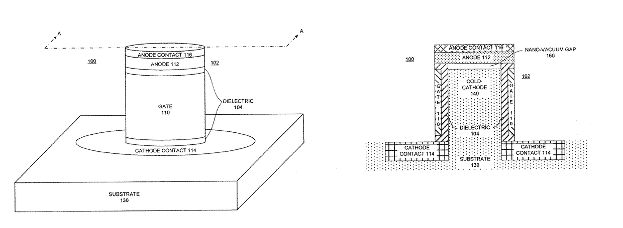
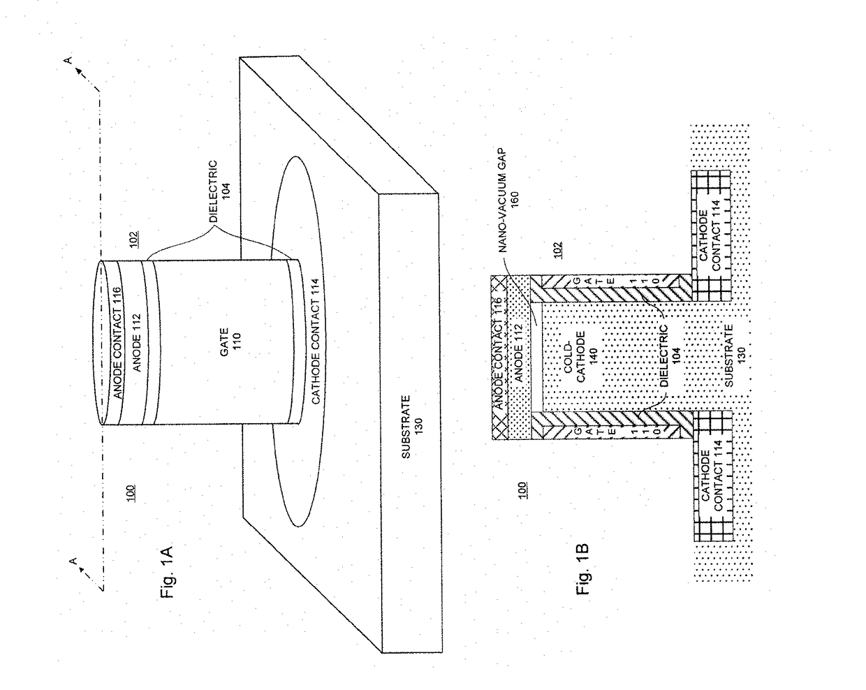
[0024]FIG. 1A is an oblique view illustration of a vacuum gap power handing device 100 in accordance with principles of the present invention, and FIG. 1B is a cross-sectional view of the vacuum gap power handling device 100 of FIG. 1A along section A-A. In FIG. 1A, a cathode pillar 140 is fabricated from a substrate 130 which may be Si, GaN, diamond, SiC or other similar materials. Other examples include taking a silicon substrate and depositing other suitable materials such as nano-crystalline diamond to form a cathode out of diamond layer. In FIG. 1A, the cathode pillar 140 is cylindrical wit...


PUM


Abstract

A semiconductor power handling device, includes a cathode pillar, a gate surrounding the cathode pillar, and an anode spaced from the cathode by a nano-vacuum gap. An array of semiconductor power handling devices, each comprising a cathode pillar, a gate surrounding the cathode pillar, and an anode spaced from the cathode pillar by a nano-vacuum gap. The semiconductor power handling devices can be arranged as rows and columns and can be interconnected to meet the requirements of various applications. The array of power handling devices can be fabricated on a single substrate.

Description

CROSS-REFERENCE TO RELATED APPLICATIONS[0001]This application claims the benefit of U.S. Provisional Patent Application No. 62 / 147,284, filed Apr. 14, 2015, which is incorporated herein by reference in its entirety.BACKGROUND OF THE INVENTION[0002]Field of the Invention[0003]The present invention relates to a nano vacuum gap power switching semiconductor device, and in particular to a device which has improved frequency range, reduced noise and increased power handling capability facilitated by the gate all-around cathode design and a nano scale vacuum gap design.[0004]Discussion of the Prior Art[0005]Vacuum gap power handling devices are known. Such devices consist of a cathode, an anode spaced apart from the cathode, and a control electrode (often called Gate) adjacent the cathode and the anode. In general, the cathode is a pointed structure from which electrons are emitted when subjected to an electric field of sufficient strength. The anode provides the necessary electric field,...

Claims


Application Information

Patent Timeline
Patent Type & Authority Patents(United States)
IPC IPC(8): H01J1/62H01J1/308H01J1/304H01J9/02H01J21/10
CPCH01J1/308H01J21/10H01J9/025H01J1/304H01J19/24H01J21/105H01J2209/0223
Inventor HUANG, BIQINROPER, CHRISTOPHER S.HUSSAIN, TAHIR
Owner HRL LAB
Why Eureka
Try Eureka