
Silicon buried digit line access device and method of forming the same

a technology of access device and digit line, which is applied in the direction of semiconductor device, semiconductor/solid-state device details, electrical apparatus, etc., can solve the problems of significant sense margin loss, several drawbacks of current bdl technology, etc., and achieve the effect of reducing dl-dl capacitance, improving the quality of components, and reducing even further dl-dl capacitan

Active Publication Date: 2017-06-27
NAN YA TECH
View PDF13 Cites 5 Cited by
  • Summary
  • Abstract
  • Description
  • Claims
  • Application Information

AI Technical Summary

Benefits of technology

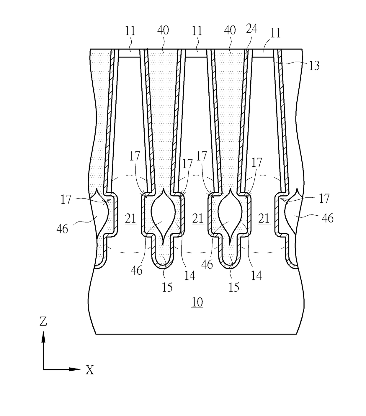
The present invention introduces a new design for semiconductor devices by eliminating a metal digit line and relying on heavily doped Si as the digit line. This reduces the DL-DL capacitance, improves component quality. Additionally, the invention provides a process flow to form airgaps between the digit lines to further decrease the capacitance. This results in a significantly improved performance of the semiconductor device and simplifies the manufacturing process, reducing costs.

Problems solved by technology

A continuous challenge in the semiconductor memory industry is to decrease the size of memory cell components in order to increase the packing density of the DRAM chips.
However, the current BDL technology still has several drawbacks.
The high percentage of DL-DL coupling causes significant sense margin loss even though the total digit line capacitance may be lower than in other technologies.

Method used


Image

  • Silicon buried digit line access device and method of forming the same
  • Silicon buried digit line access device and method of forming the same
  • Silicon buried digit line access device and method of forming the same

Examples


Embodiment Construction

[0015]In the following detailed description of the invention, reference is made to the accompanying drawings, which form a part hereof, and in which is shown, by way of illustration, specific embodiments in which the invention may be practiced. These embodiments are described in sufficient detail to enable those skilled in the art to practice the invention. Other embodiments may be utilized and structural, logical, and electrical changes may be made without departing from the scope of the present invention. Most of the processes utilized in the present invention are well known to those skilled in the art and are not explicitly described or detailed.

[0016]In a preferred embodiment of present invention, a substrate 10 is provided. In this substrate, an area is defined to implement the array of the next steps through a first process. The substrate 10 may be a silicon substrate. Shallow Trench Isolations (STI) are formed in the substrate 10 to define a periphery of the device of the pre...


PUM


Abstract

An access device includes a plurality of first digit lines (DL) trenches extending along a first direction, buried digit lines between each DL trench, second and third trenches separating the digit lines, a filling material filling the digit line trenches comprising airgaps in each second trench, a plurality of word line (WL) trenches extending along a second direction, metal word lines deposited on the walls of the word line trenches, a filling material filling the word line trenches.

Description

BACKGROUND OF THE INVENTION[0001]1. Field of the Invention[0002]The present invention relates generally to the field of integrated circuit fabrication and, more particularly, to a silicon buried digit line (BDL) access device for memories such as DRAM, wherein the buried digit lines are separated with air gaps.[0003]2. Description of the Prior Art[0004]A continuous challenge in the semiconductor memory industry is to decrease the size of memory cell components in order to increase the packing density of the DRAM chips. Over the last few device generations, DRAM manufacturers have developed alternative cell layouts that reduce the area occupied by the memories on chips. The latest designs allow a significant increase in density by burying the address lines or digit lines into the silicon substrate, then fabricating the transistors and capacitors on top to form a vertical stack. Such devices are also known as buried digit line (BDL) access devices.[0005]However, the current BDL techno...

Claims


Application Information

Patent Timeline
Patent Type & Authority Patents(United States)
IPC IPC(8): H01L29/78H01L27/108H01L23/522H10B12/00
CPCH01L27/10891H01L23/5222H01L27/10885H01L2924/0002H10B12/488H10B12/482H01L2924/00
Inventor SURTHI, SHYAMHEINECK, LARS
Owner NAN YA TECH
Learn More