
Nonvolatile static random access memory (NVSRAM) system having a static random access memory (SRAM) array and a resistive memory array

a static random access memory and array technology, applied in the field of memory systems, can solve the problems of inefficient area and slow read and write access times of resistive memories

Active Publication Date: 2017-05-02
NXP USA INC
View PDF7 Cites 17 Cited by
  • Summary
  • Abstract
  • Description
  • Claims
  • Application Information

AI Technical Summary

Benefits of technology

The present invention is about a system that combines a discrete SRAM array and a resistive memory array to provide a non-volatile memory system that is area efficient. The system includes a sense amplifier that is shared between the two memories and is used for both read and write operations. The system also includes a calibration phase and a non-calibration phase for the resistive memory, and the system is designed to provide the appropriate store and restore functionality in an area efficient manner. The technical effect of the invention is to provide a tightly coupled NVSRAM system that provides the appropriate store and restore functionality in an area efficient manner.

Problems solved by technology

However, read and write access times for resistive memories are typically slow, especially as compared to read and write access times for SRAMs.
Alternative solutions includes memory cells which have both volatile and non-volatile portions, but these are area inefficient.

Method used


Image

  • Nonvolatile static random access memory (NVSRAM) system having a static random access memory (SRAM) array and a resistive memory array
  • Nonvolatile static random access memory (NVSRAM) system having a static random access memory (SRAM) array and a resistive memory array
  • Nonvolatile static random access memory (NVSRAM) system having a static random access memory (SRAM) array and a resistive memory array

Examples


Embodiment Construction

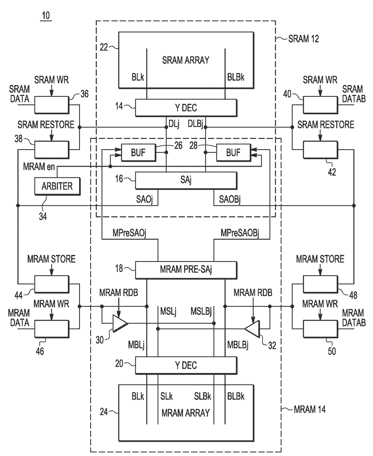
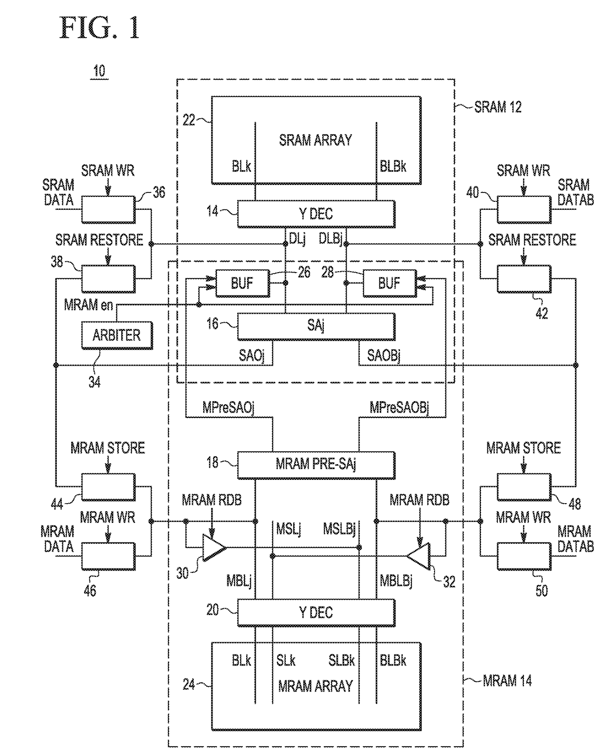
[0009]A NVSRAM system includes a discrete SRAM array and resistive memory array used to store and restore backup data. Data is stored from the SRAM array to the resistive memory array for backup and restored back from the resistive memory array to the SRAM array for normal operation. In order to gain area efficiency, the resistive memory array and SRAM array share the sense amplifiers. For an SRAM read operation, the sense amplifiers are used to provide the output data. In one embodiment, the resistive memory array is an MRAM array. An MRAM read operation includes two phases: a calibration phase and a non-calibration (i.e. sense) phase. For an MRAM read operation, the sense amplifiers are also used for the non-calibration phase to provide the output data. In this manner, a tightly coupled NVSRAM system provides the appropriate store and restore functionality in an area efficient manner.

[0010]FIG. 1 illustrates an NVSRAM system 10 in accordance with one embodiment of the present inve...


PUM


Abstract

An integrated circuit (IC) device includes a static random access memory (SRAM) array, and a resistive memory (resistive memory) array. A first set of programmable resistive elements in the resistive memory array are used to store data from memory cells in the SRAM array. Sense amplifier circuitry is couplable to the SRAM array and the resistive memory array. An arbiter is configured to assert an resistive memory enable signal to couple the sense amplifier circuitry to the resistive memory array and decouple the sense amplifier circuitry from the SRAM array during a resistive memory read operation, and to couple the sense amplifier to the SRAM array and decouple the sense amplifier circuitry from the resistive memory array during an SRAM read operation.

Description

BACKGROUND[0001]Field[0002]This disclosure relates generally to memory systems, and more specifically, to memory systems having an SRAM array and a resistive memory array.[0003]Related Art[0004]Resistive memories, such as magnetoresistive RAMs (MRAMs), are commonly used non-volatile memories. However, read and write access times for resistive memories are typically slow, especially as compared to read and write access times for SRAMs. Therefore, in some systems, non-volatile memory (NVM) backup to SRAM is used. In such systems, an SRAM is used for operation on the data, and upon power down, the data is moved from SRAM to a NVM, such as MRAM. The data is then restored back to the SRAM upon powering up. This solution provides the operation efficiency offered by SRAMs and the non-volatility provided by MRAMs. Such a system may be referred to as a non-volatile SRAM (NVSRAM). In one NVSRAM solution, a bus interface between the two memories is required which must switch during data transf...

Claims


Application Information

Patent Timeline
Patent Type & Authority Patents(United States)
IPC IPC(8): G11C8/00G11C11/16G11C11/419G11C14/00H01L27/11H01L27/24H10B10/00
CPCG11C14/0081H01L27/1112H01L27/2436G11C11/419G11C11/1673G11C7/1051G11C7/1078G11C11/16G11C11/413G11C11/005G11C13/004G11C27/024G11C2013/0042G11C2013/0045H10B10/12
Inventor ROY, ANIRBANCHOY, JON S.SADD, MICHAEL A.
Owner NXP USA INC
Learn More