Manufacturing method for component incorporated substrate and component incorporated substrate

a manufacturing method and technology for components, applied in sustainable manufacturing/processing, final product manufacturing, semiconductor/solid-state device details, etc., can solve the problems of deterioration of the connection section between the wiring pattern and the terminal section of the electronic component, and achieve accurate positioning of the component, accurate contour specification, and improved detection accuracy

Inactive Publication Date: 2017-04-11
MEIKO ELECTRONICS CO LTD
View PDF16 Cites 0 Cited by
  • Summary
  • Abstract
  • Description
  • Claims
  • Application Information

AI Technical Summary

Benefits of technology

[0016]In the manufacturing method for the component incorporated substrate according to the present invention, in the mark forming step, when an imaginary line extending from a search center, which is the center of the search range of the detecting means, to the edge side of the search range is represented as a search reference line and an imaginary line extending, in a state in which the center of the mark is matched with the search center, from the center of the mark in the same direction as the search reference line and to an outer ridgeline, which is the boundary between the top surface and the outer circumferential curved surface in the mark, is represented as a mark reference line, the mark is formed in a shape in which the outer ridgeline of the mark is present in a position where the length of the mark reference line is in a range of 30% or more of the search reference line. Therefore, effects described below are attained. That is, since a ratio of the mark in the search range increases, it is possible to accurately perform specifying of the contour of the mark. Consequently, it is possible to improve detection accuracy of the mark and accurately perform positioning of the component and specifying of the position of the component.
[0017]Since the component incorporated substrate of the present invention is obtained by the manufacturing method explained above, detection accuracy of the mark is high, the terminal of the incorporated component and the wiring pattern are highly accurately positioned, failures of electrical connection are extremely few, and the component incorporated substrate is excellent in quality.

Problems solved by technology

Therefore, it is likely that reliability of the connecting section between the wiring pattern and the terminal section of the electronic component is deteriorated.

Method used


Image

  • Manufacturing method for component incorporated substrate and component incorporated substrate
  • Manufacturing method for component incorporated substrate and component incorporated substrate
  • Manufacturing method for component incorporated substrate and component incorporated substrate

Examples


first embodiment

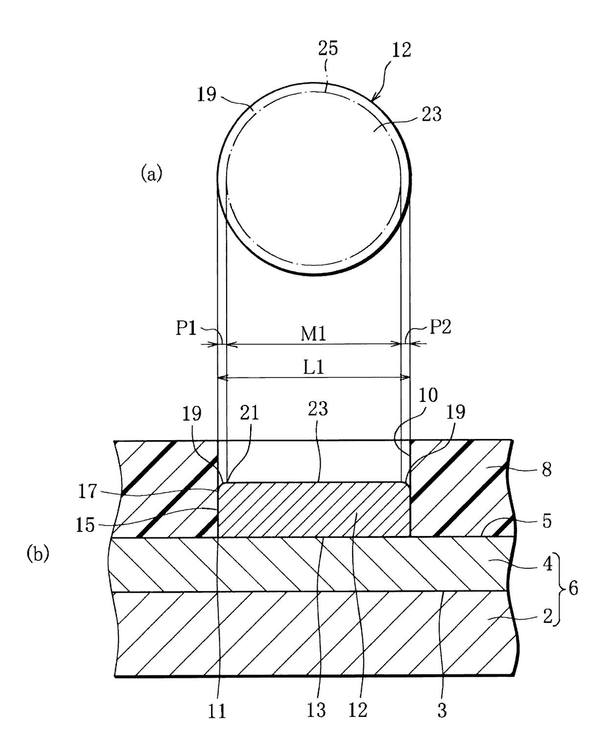
[0039]In the present invention, first, a mark for positioning consisting of a columnar body made of copper is formed on a starting material (a mark forming step). The starting material is prepared, for example, as explained below.

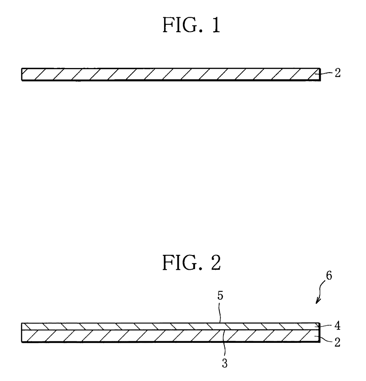
[0040]First, as shown in FIG. 1, a supporting plate 2 is prepared. The supporting plate 2 is, for example, a thin plate made of stainless steel. As shown in FIG. 2, a first copper layer 4 consisting of a thin film is formed on the supporting plate 2. The first copper layer 4 consists of, for example, a copper plating film obtained by electroplating. A copper-plated steel plate 6 obtained in this way is used as a starting material. In the first copper layer 4, a surface in contact with the supporting plate 2 is represented as a first surface 3. A surface on the opposite side of the first surface 3 is represented as a second surface 5.

[0041]Note that, as the supporting plate 2, a thin plate made of aluminum can be used. In this case, the first copper layer 4 ...

second embodiment

[0078]A second embodiment is different from the first embodiment only in that a mark 90, a plan view shape of which is square, shown in FIG. 18 is formed in the mark forming step in the first embodiment.

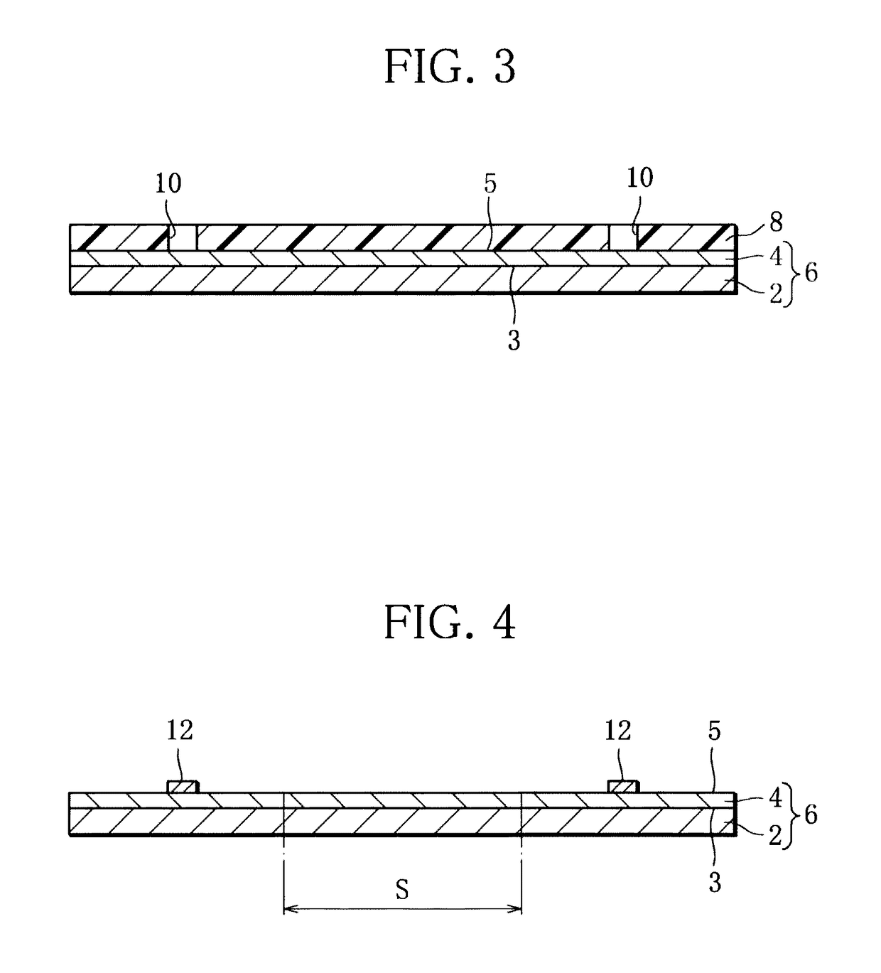
[0079]In the mark forming step in the second embodiment, first, as shown in FIG. 18(b), the mask layer 8 is formed on the first copper layer 4 of the prepared copper-plated steel plate 6. In the mask layer 8, an opening 92 consisting of a through-hole, a plan view shape of which is square, is provided in a predetermined position. Electroplating of copper is applied to the copper-plated steel plate 6 including such a mask layer 8 to form a copper plated layer in the opening 92. Consequently, as shown in FIG. 18(a), the mark 90, the plan view shape of which is square, is obtained. As it is evident from FIG. 18, an outer ridgeline 94 of the mark 90 is formed in a square shape and is located further on the outer side than the lower limit region 84.

[0080]In this embodiment, an optical sys...

third embodiment

[0081]A third embodiment is different from the first embodiment only in that a ring-like mark 100, a plan view shape of which is circular, shown in FIG. 19 is formed in the mark forming step in the first embodiment.

[0082]In the mark forming step in the third embodiment, first, as shown in FIG. 19(b), the mask layer 8 is formed on the first copper layer 4 of the prepared copper-plated steel plate 6. In the mask layer 8, an opening 102 consisting of a ring-like through-hole, a plan view shape of which is circular, is provided in a predetermined position. Electroplating of copper is applied to the copper-plated steel plate 6 including such a mask layer 8 to form a copper plated layer in the opening 102. Consequently, as shown in FIG. 19(a), the ring-like mark 100, the plan view shape of which is circular, is obtained. As it is evident from FIG. 19, an outer ridgeline 104 of the mark 100 is formed in a circular shape and is located further on the outer side than the lower limit region 8...


PUM

PropertyMeasurementUnit
lengthaaaaaaaaaa
lengthaaaaaaaaaa
widthsaaaaaaaaaa

Abstract

In a mark forming step in a manufacturing method for a component incorporated substrate in which an electronic component is positioned with reference to a mark formed in a copper layer, when an imaginary line extending from a search center of a search range of a sensor, to an edge side of the search range is represented as a search reference line and an imaginary line extending, in a state in which a mark center, is matched with the search center, from the mark center in the same direction as the search reference line to an outer ridgeline of the mark is represented as a mark reference line, the mark formed in a shape in which the outer ridgeline of the mark is present in a position where a length of the mark reference line is in a range of 30% or more of the search reference line.

Description

TECHNICAL FIELD[0001]The present invention relates to manufacturing method for a component incorporated substrate in which electric or electronic components are embedded in a substrate and a component incorporated substrate manufactured using the method.BACKGROUND ART[0002]In recent years, according to an increase in density and improvement of functions of electronic circuit substrate, a component incorporated substrate having structure in which electronic components are embedded in an insulating substrate which is an insulating layer has been attracting attention (see, for example, Patent Document 1). In such a component incorporated substrate, a wiring pattern is formed on the surface of the insulating substrate. The component incorporated substrate can be used as a module with other various electronic components surface-mounted in predetermined positions of the wiring pattern. The component incorporated substrate can also be used as a core substrate in manufacturing a component i...

Claims


Application Information

Patent Timeline
Patent Type & Authority Patents(United States)
IPC IPC(8): H05K3/30H05K1/18H05K1/02H05K1/09H05K1/11
CPCH05K1/188H05K1/0269H05K1/0284H05K1/09H05K1/115H05K3/305H05K2201/0335H05K2201/09918Y10T29/49131H01L21/568H01L21/6835H01L23/544H01L24/19H01L24/27H01L24/29H01L24/32H01L24/82H01L24/83H01L24/92H01L2221/68359H01L2223/54426H01L2223/54486H01L2224/04105H01L2224/2741H01L2224/27436H01L2224/2919H01L2224/2929H01L2224/29387H01L2224/32245H01L2224/82039H01L2224/82132H01L2224/83005H01L2224/83132H01L2224/8314H01L2224/83192H01L2224/92144H01L2924/14H05K3/4007H05K2201/09154H05K2201/0939H05K2201/09472H05K2203/0353H05K2203/0361H05K2203/063Y02P70/50
Inventor SHIMIZU, RYOICHIIWAMOTO, MITSUOTODA, MITSUAKI
Owner MEIKO ELECTRONICS CO LTD
Why Eureka
Try Eureka