Method for forming patterns for semiconductor device

a semiconductor device and pattern technology, applied in semiconductor/solid-state device manufacturing, basic electric elements, electric devices, etc., can solve the problems of smaller feature size and complicated pattern including features, and achieve the effect of ensuring process yield

Active Publication Date: 2017-01-03
UNITED MICROELECTRONICS CORP
View PDF5 Cites 0 Cited by
  • Summary
  • Abstract
  • Description
  • Claims
  • Application Information

AI Technical Summary

Benefits of technology

[0007]According to the method for forming patterns for semiconductor device provided by the present invention, the desirable / object patterns are decomposed into the spacer patterns, the first blocking layers and the second blocking layers. With the spacer patterns, the first blocking layers, and the second blocking layers serving as masks, the hard mask layer is patterned and thus the patterned hard mask layer is obtained. Therefore, the patterned hard mask layer includes the desirable / object patterns transferred from the spacer patterns, the first blocking layers and the second blocking layers. Accordingly, the method for forming the patterns for semiconductor device provide by the present invention is able to precisely and accurately form the required fine features and thus process yield is ensured.

Problems solved by technology

That is, the feature size becomes smaller while the pattern including those features becomes more and more complicated.

Method used


Image

  • Method for forming patterns for semiconductor device
  • Method for forming patterns for semiconductor device
  • Method for forming patterns for semiconductor device

Examples


Embodiment Construction

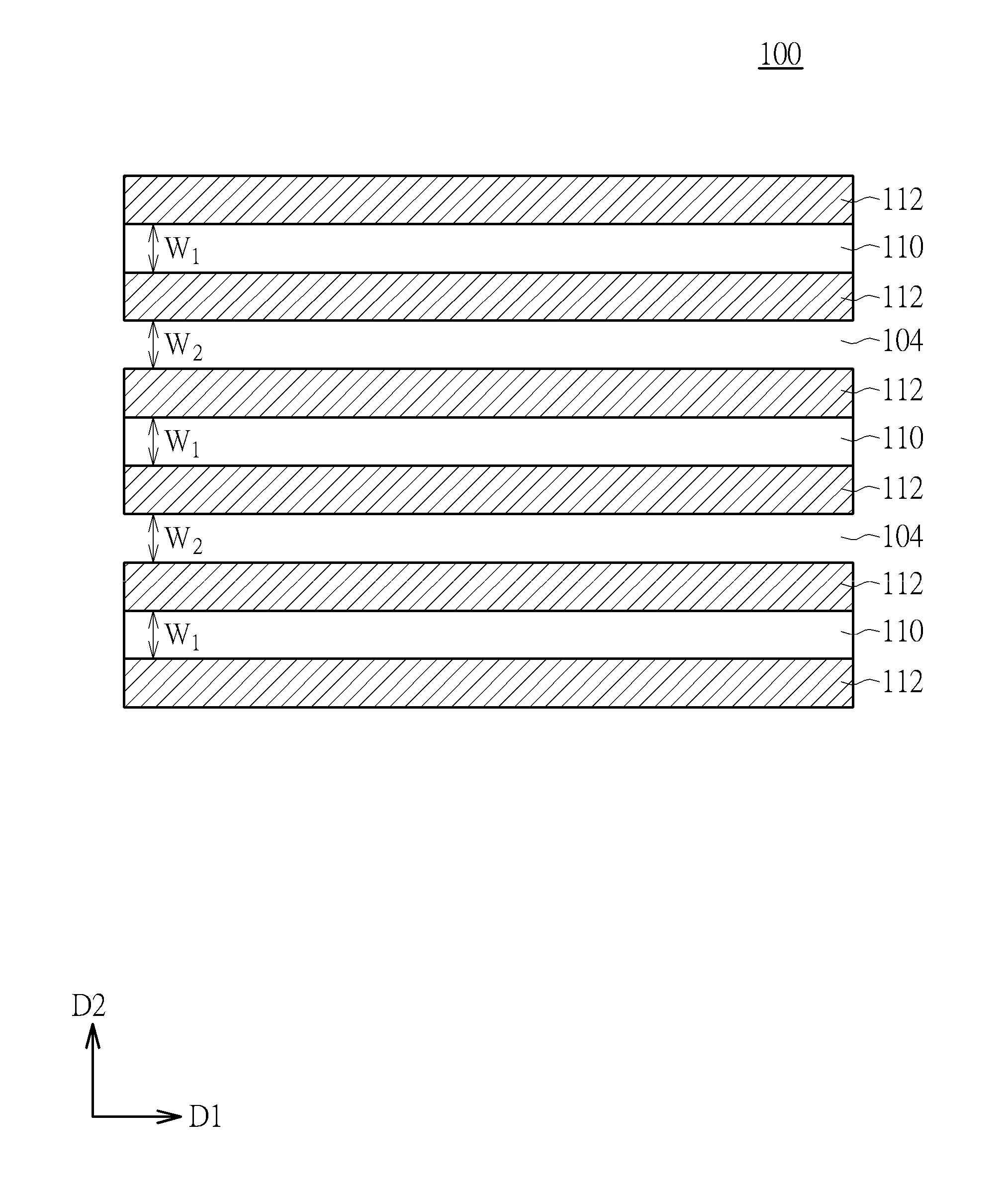
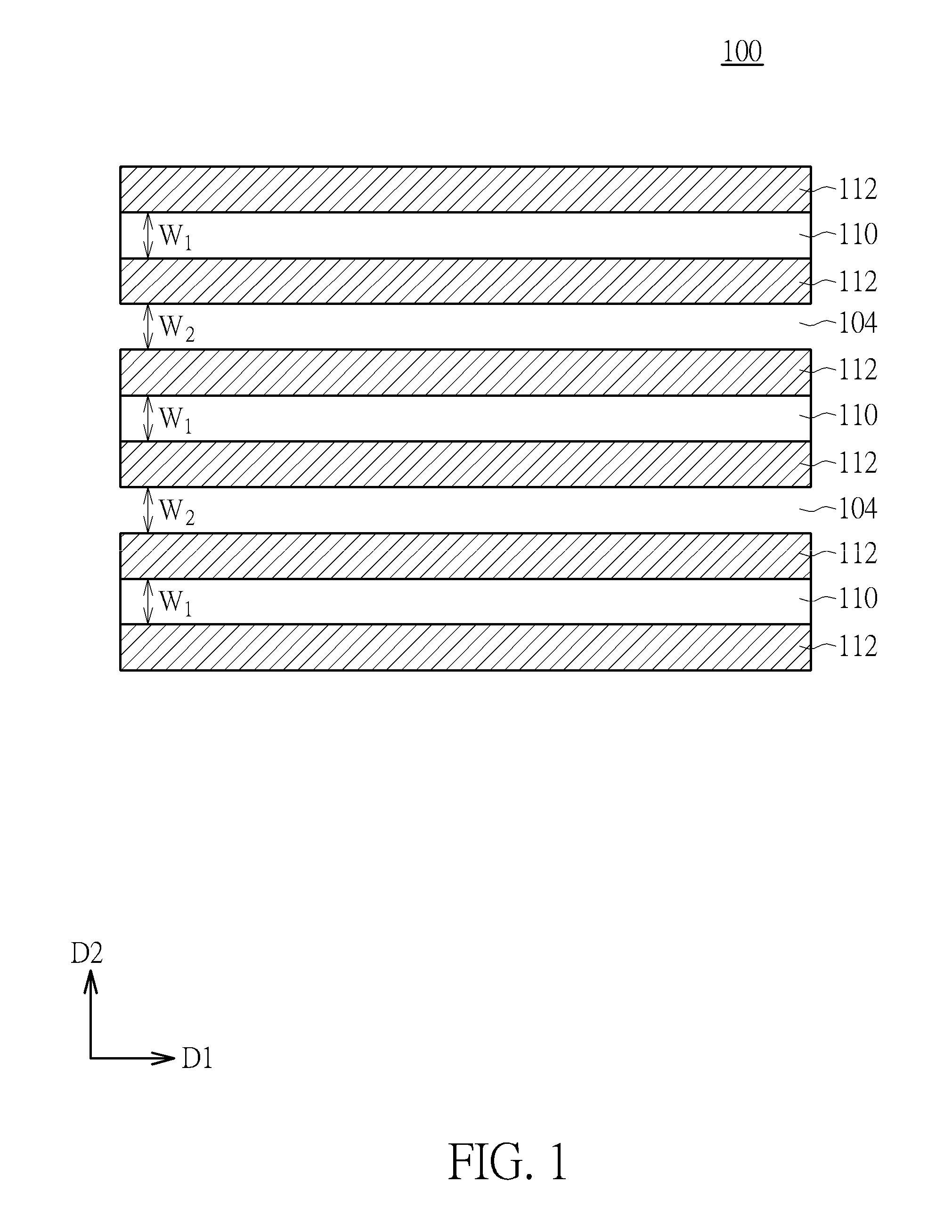
[0011]Please refer to FIGS. 1-7B, which are schematic drawings illustrating a method for forming patterns for semiconductor device provided by a first preferred embodiment of the present invention. FIG. 2B is a cross-sectional view taken along a line A-A′ of FIG. 2A, and FIGS. 3B-7B respectively are cross-sectional views taken along a line B-B′ of FIGS. 3A-7A. As shown in FIG. 1, the preferred embodiment first provides a substrate 100, such as a silicon substrate. The substrate 100 can include a silicon-on-insulator (hereinafter abbreviated as SOI) substrate or a bulk silicon substrate if required. Furthermore, the substrate 100 can even include dielectric layer if required, but not limited to this. It is therefore concluded that the substrate 100 provided by the preferred embodiment can be any suitable substrate or lamination capable of accommodating semiconductor IC elements. The substrate 100 includes at least a hard mask layer 102 (shown in FIG. 2B) and a sacrificial layer 104 f...


PUM


Abstract

A method for forming patterns for semiconductor device includes following steps. A substrate is provided. The substrate includes a hard mask layer and a sacrificial layer formed thereon. A plurality of spacer patterns parallel with each other are formed on the substrate. A plurality of first blocking layers are formed in the sacrificial layer after forming the spacer patterns. A plurality of second blocking layers exposing at least a portion of the sacrificial layer and at least a portion the first blocking layer are formed on the substrate after forming the first blocking layer. Next, the sacrificial layer and the hard mask layer are etched with the spacer patterns, the first blocking layers and the second blocking layer being used as etching masks to form a patterned hard mask layer on the substrate.

Description

BACKGROUND OF THE INVENTION[0001]1. Field of the Invention[0002]The present invention relates to a method for forming patterns for semiconductor device, and more particularly, to a method for forming semiconductor device involved with multiple patterning technique.[0003]2. Description of the Prior Art[0004]Photolithography is one of the basic processes used for manufacturing semiconductor devices which construct integrated circuits (ICs) in semiconductor factory. When fabricating those semiconductor devices, wafer / substrate or layers formed on substrate is / are patterned to create geometric features for realizing the elements that are to form the devices. As semiconductor manufacturing processes continue to advance, the dimensions of circuit elements have continually been reduced while the amount of functional elements, such as transistors, has been steadily increasing over decades. That is, the feature size becomes smaller while the pattern including those features becomes more and ...

Claims


Application Information

Patent Timeline
Patent Type & Authority Patents(United States)
IPC IPC(8): H01L21/308H01L21/768
CPCH01L21/3088H01L21/3081H01L21/3085H01L21/3086H01L21/76816H01L21/76877H01L21/0332H01L21/0337H01L21/0338H01L21/31144H01L21/0273
Inventor FU, TZU-HAOCHENG, HOME-BEENCHU, CI-DONGHSIEH, TSUNG-YIN
Owner UNITED MICROELECTRONICS CORP
Why Eureka
Try Eureka