Variable matching circuit and amplifier
a matching circuit and amplifier technology, applied in the direction of low noise amplifiers, amplifiers using switched capacitors, gain control, etc., can solve the problems of significant influence of performance degradation of transistors as amplifying elements used in low noise amplifiers, performance degradation of receivers, etc., to reduce reflection of high frequency signals, improve noise figures, and reduce loss
- Summary
- Abstract
- Description
- Claims
- Application Information
AI Technical Summary
Benefits of technology
Problems solved by technology
Method used
Image
Examples
first embodiment
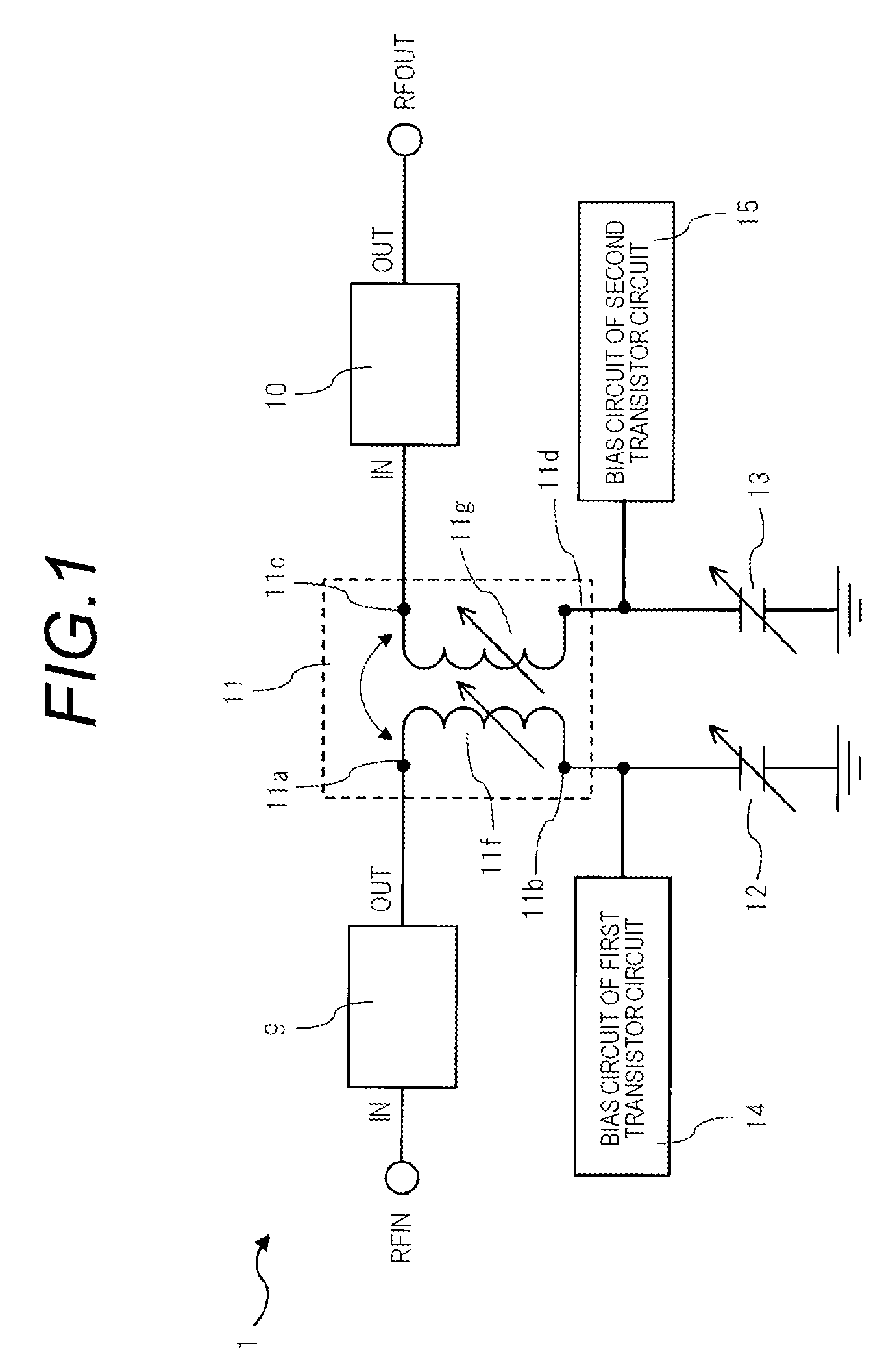
[0048]FIG. 1 is a diagram illustrating an internal configuration of a variable matching circuit 1 according to a first embodiment. The variable matching circuit 1 illustrated in FIG. 1 includes a first transistor circuit 9, a second transistor circuit 10, a transformer 11, a first capacitive element 12, and a second capacitive element 13. Furthermore, the variable matching circuit 1 may further include a bias circuit 14 for the first transistor circuit, and a bias circuit 15 for the second transistor circuit.
[0049]The first transistor circuit 9 is operated by a DC power source voltage supplied from the bias circuit 14 for the first transistor circuit, amplifies a high frequency signal input to an input terminal RFIN, and outputs the signal to a primary inductor device 11f of the transformer 11.
[0050]The second transistor circuit 10 is operated by a DC power source voltage supplied from a power source voltage generating circuit (not illustrated), and the high frequency signal amplifi...
modification example of first embodiment
[0086]FIG. 7 is a diagram illustrating an internal configuration of a variable matching circuit 1A according to a modification example of the first embodiment. In the variable matching circuit 1A of this modification example, as the bias circuit 14 for the first transistor circuit in the variable matching circuit 1 illustrated in FIG. 1, a choke coil 16a and a variable voltage source 17a are illustrated, and as the bias circuit 15 for the second transistor circuit, a choke coil 16b and a variable voltage source 17b are illustrated.
[0087]One end of the choke coil 16a is connected to the terminal 11b, the other end thereof is connected to the variable voltage source 17a, and the choke coil 16a transmits a DC potential by being open in terms of AC.
[0088]One end of the choke coil 16b is connected to the terminal 11d, the other end thereof is connected to the variable voltage source 17b, and the choke coil 16b transmits the DC potential by being open in terms of AC.
[0089]The variable vol...
second embodiment
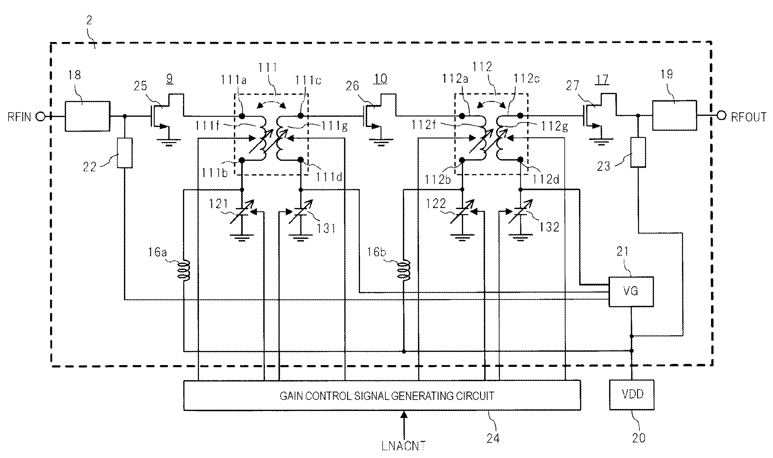
[0097]In the second embodiment, a circuit configuration of the amplifier using the variable matching circuit 1 according to the first embodiment will be described. Furthermore, the same configurations as those of the variable matching circuit 1 according to the first embodiment are represented by the same reference numerals or signs, the description thereof will be omitted or simplified, and different configurations will be described. FIG. 9 is a diagram illustrating a circuit configuration of an amplifier 2 according to the second embodiment. The amplifier 2 is used, for example, as a low noise amplifier (LNA) connected to a following stage of a receiving antenna.
[0098]The amplifier 2 illustrated in FIG. 9 includes an input matching circuit 18, a DC potential transmission circuit 22, two variable matching circuits 1 (refer to FIG. 1), an output matching circuit 19, a DC potential transmission circuit 23, and a DC control voltage generating circuit 21. Among the two variable matchin...
PUM
 Abstract
Description
Claims
Application Information
 - R&D
- Intellectual Property
- Life Sciences
- Materials
- Tech Scout
- Unparalleled Data Quality
- Higher Quality Content
- 60% Fewer Hallucinations
Browse by: Latest US Patents, China's latest patents, Technical Efficacy Thesaurus, Application Domain, Technology Topic, Popular Technical Reports.
© 2025 PatSnap. All rights reserved.Legal|Privacy policy|Modern Slavery Act Transparency Statement|Sitemap|About US| Contact US: help@patsnap.com


