
Hybrid computing module

a computing module and hybrid technology, applied in the field of customized system construction, can solve the problems of limiting the industry's options, high foundry costs, and exponential growth of design, mask and fabrication costs, so as to reduce the size and cost of computing systems, reduce the effect of data transfer efficiency and increase performan

Active Publication Date: 2016-05-24
DEROCHEMONT L PIERRE
View PDF25 Cites 15 Cited by
  • Summary
  • Abstract
  • Description
  • Claims
  • Application Information

AI Technical Summary

Benefits of technology

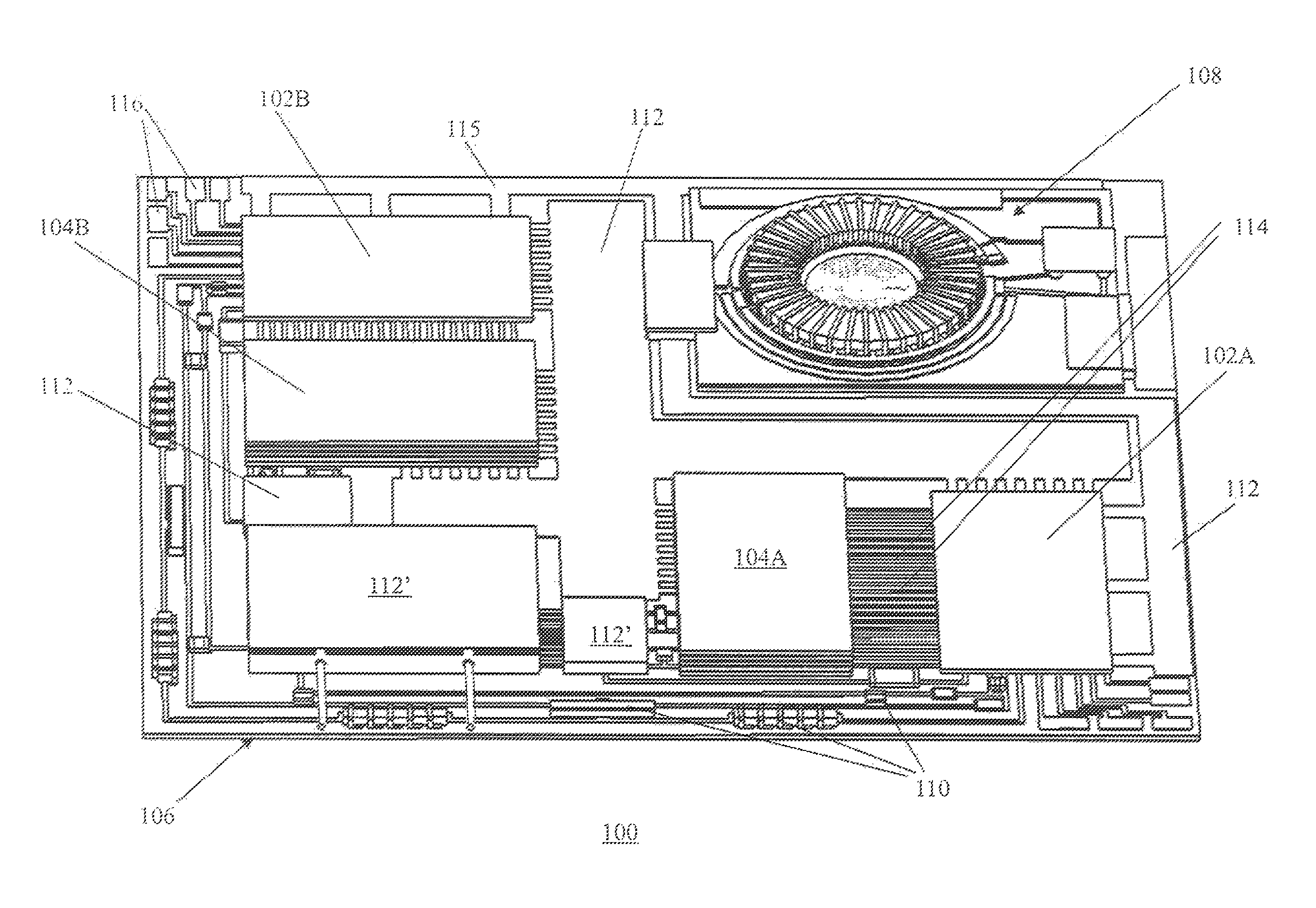
[0049]The present invention generally relates to a hybrid system-on-chip that comprises a plurality of memory and processor die mounted on a semiconductor carrier chip that contains a fully integrated power management system that switches DC power at speeds that match or approach processor core clock speeds, thereby allowing the efficient transfer of data between off-chip physical memory and processor die. The present invention relates to methods and means to reduce the size and cost of computing systems, while increasing performance. The present invention relates to methods and means to provide a factor increase in computing performance per processor die surface area while only fractionally increasing power consumption.

Problems solved by technology

While this path has led to exponential growth in computing performance, and substantial reductions in chip unit costs, Moore's Law has had some consequences that have started restricting the industry's options.
First, the design, mask, and fabrication costs have grown exponentially.
Secondly, limitations related to the long design times and extremely high foundry costs have thinned the number of chip producers in the marketplace.
It is now generally accepted that in 2015, it will no longer be possible to supply sufficient power to multi-core microprocessors to drive all the transistors and higher speeds.
While this will not allow all transistor to be operating simultaneously, nor will it allow them all to operating at higher speeds, this proposed solution will keep pace with the exponential growth curve the industry is accustomed to.
The problem with this solution will be marketplace acceptance.
While elegant, this solution failed for several reasons.
First, the marketplace was too fragmented for a one-size-fits-all solution.
Secondly, the marketplace was changing too fast to digest the 2-year minimum design cycles needed to produce the one-size-fits-all solution.

Method used


Image

  • Hybrid computing module
  • Hybrid computing module
  • Hybrid computing module

Examples


Embodiment Construction

[0087]The present invention is illustratively described above in reference to the disclosed embodiments. Various modifications and changes may be made to the disclosed embodiments by persons skilled in the art without departing from the scope of the present invention as defined in the appended claims.

[0088]This application incorporates by reference all matter contained in de Rochemont U.S. Pat. No. 7,405,698 entitled “CERAMIC ANTENNA MODULE AND METHODS OF MANUFACTURE THEREOF” (the '698 application), de Rochemont U.S. Ser. No. 11 / 479,159, filed Jun. 30, 2006, entitled “ELECTRICAL COMPONENT AND METHOD OF MANUFACTURE” (the '159 application), U.S. Ser. No. 11 / 620,042 (the '042 application), filed Jan. 6, 2007 entitled “POWER MANAGEMENT MODULES”, de Rochemont and Kovacs, “LIQUID CHEMICAL DEPOSITION PROCESS APPARATUS AND EMBODIMENTS”, U.S. Ser. No. 12 / 843,112, ('112), de Rochemont, “MONOLITHIC DC / DC POWER MANAGEMENT MODULE WITH SURFACE FET”, U.S. Ser. No. 13 / 152,222 ('222), de Rochemont, ...


PUM


Abstract

A hybrid system-on-chip provides a plurality of memory and processor die mounted on a semiconductor carrier chip that contains a fully integrated power management system that switches DC power at speeds that match or approach processor core clock speeds, to enable transfer of data between off-chip physical memory and processor die.

Description

CROSS REFERENCE TO RELATED APPLICATIONS[0001]This application claims priority from U.S. Provisional Patent Application Ser. No. 61 / 669,557, filed Jul. 9, 2012 and from U.S. Provisional Patent Application Ser. No. 61 / 776,333, filed Mar. 11, 2013, both of which are incorporated herein by reference in their entirety.FIELD OF THE INVENTION[0002]The present invention relates generally to the construction of customized system-on-chip computing modules and specifically to the application of semiconductor carriers comprising a fully integrated power management system that transfers data between at least one memory die mounted on the semiconductor carrier at speeds that are synchronous or comparable with at least one general purpose processor die co-located on the semiconductor carrier.[0003]The present invention relates generally to methods and means that reduce the physical size and cost of high-speed computing modules. More specifically, the present invention instructs methods and means t...

Claims


Application Information

Patent Timeline
Patent Type & Authority Patents(United States)
IPC IPC(8): G06F12/00H01L25/16H01L21/84G06F1/32G06F1/26H01L21/762H01L21/00H01L27/02H01L25/065
CPCG06F1/26G06F1/3203H01L21/00H01L21/76229H01L21/84H01L25/16H01L27/0207H01L25/0652H01L2924/0002H01L2924/14H01L2924/3011Y10S257/00H01L2924/00G06F13/1605G06F13/1689G06F13/24G06F13/1673G06F13/36G06F13/42Y02D10/00G06F9/3001G06F9/30043G06F9/30098G06F9/3802G06F12/1009G06F2212/65G06F1/324G06F2213/0038G11C7/1072G06F1/28G06F12/0815G06F12/0862G06F12/0875G06F15/80G06F2212/1024G06F2212/452G06F2212/602G06F2212/621G06F3/0619G06F3/0625G06F3/065G06F3/0685
Inventor DE ROCHEMONTKOVACS, ALEXANDER J.
Owner DEROCHEMONT L PIERRE
Learn More