Electrophotographic photoreceptor and image forming apparatus including the same
a photoreceptor and photoreceptor technology, applied in the field of electrotrophotographic photoreceptor and image forming apparatus, can solve the problems of inhibiting sensitivity reduction, deterioration of photoreceptor electric properties, and insufficient dispersion stability, so as to improve dispersion stability, improve dispersion stability, and high wear resistance
- Summary
- Abstract
- Description
- Claims
- Application Information
AI Technical Summary
Benefits of technology
Problems solved by technology
Method used
Image
Examples
embodiment 1
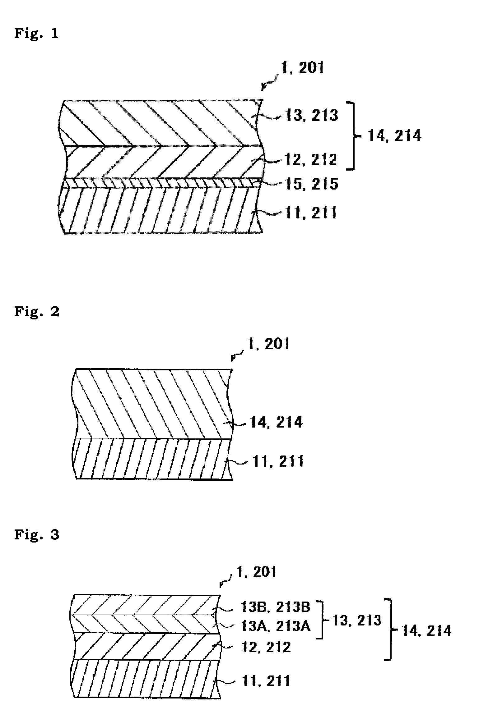
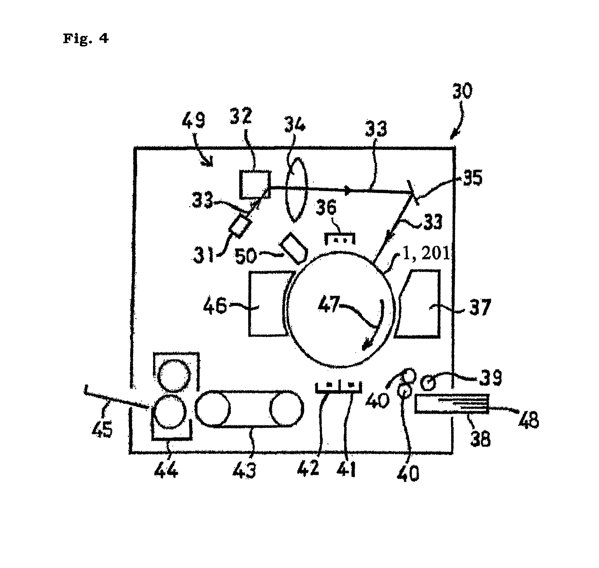
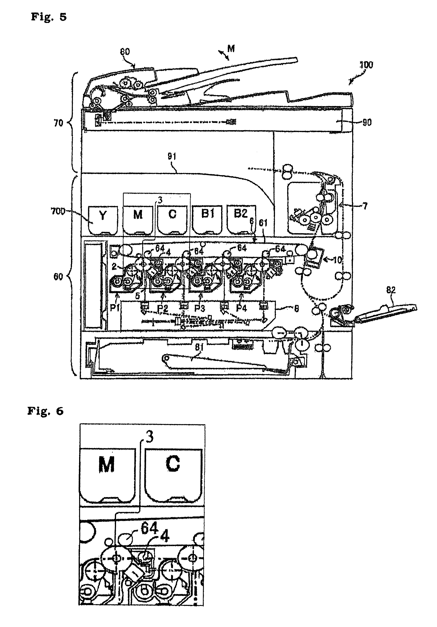
[0065]FIG. 1 is a schematic sectional view showing a configuration of an electrophotographic photoreceptor according to Embodiment 1 of the present invention. An electrophotographic photoreceptor 1, 201 according to Embodiment 1 (hereinafter, abbreviated as “photoreceptor”) is a multilayered photoreceptor including, in sequence, a cylindrical conductive substrate 11, 211 formed of a conductive material; an undercoat layer 15, 215; and a photosensitive layer 14, 214 including a charge generation layer 12, 212 containing a charge generation material and a charge transport layer 13, 213 containing a charge transport material stacked in this order.
Conductive Substrate (Hereinafter, May be Referred to as “Conductive Support”)
[0066]The conductive substrate 11, 211 plays a role as an electrode of the photoreceptor 1 and functions as a supporting member for the layers disposed thereon, that is, the undercoat layer 15, 215 and the photosensitive layer 14, 214.
[0067]While the conductive subst...
embodiment 2
[0158]As Embodiment 1, an embodiment has been described in which the photosensitive layer 14, 214 is a multilayered photosensitive layer including the charge generation layer 12, 212 and the charge transport layer 13, 213. In another embodiment, however, the photosensitive layer 14, 214 may be a single layer, that is, a monolayer photosensitive layer as shown in FIG. 2.
[0159]Specifically, the photoreceptor 1, 201 may be formed from the cylindrical conductive substrate 11, 211 made of a conductive material, and a photosensitive layer 14, 214 which is a layer stacked on an outer circumferential surface of the conductive substrate 11, 211 and which contains a charge generation material and a charge transport material.
embodiment 3
[0160]In another embodiment, the charge transport layer 13, 213 may be formed from a plurality of layers as shown in FIG. 3.
[0161]In the present embodiment, specifically, the charge transport layer is formed from two different charge transport layers 13A (213A) and 13B, 213B stacked one on top of the other, and oxygen-containing fluorinated fine particles are added to the charge transport layer 13B, 213B constituting the outermost surface. That is, FIG. 3 shows an embodiment in which the charge transport layer 13, 213 is formed from the first charge transport layer 13A, 213A and the second charge transport layer 13B, 213B, the first charge transport layer 13A, 213A and the second charge transport layer 13B, 213B have different charge transport material contents, and the second charge transport layer 13B, 213B contains filler particles.
[0162]When the charge transport layer 13, 213 is formed from a plurality of layers stacked one on top of the other as described above, filler particle...
PUM
| Property | Measurement | Unit |
|---|---|---|
| median size | aaaaa | aaaaa |
| ionization potential | aaaaa | aaaaa |
| ionization potential | aaaaa | aaaaa |
Abstract
Description
Claims
Application Information
 - R&D
- Intellectual Property
- Life Sciences
- Materials
- Tech Scout
- Unparalleled Data Quality
- Higher Quality Content
- 60% Fewer Hallucinations
Browse by: Latest US Patents, China's latest patents, Technical Efficacy Thesaurus, Application Domain, Technology Topic, Popular Technical Reports.
© 2025 PatSnap. All rights reserved.Legal|Privacy policy|Modern Slavery Act Transparency Statement|Sitemap|About US| Contact US: help@patsnap.com


