Electrode substrate and planar optoelectronic device
a technology of optoelectronic devices and electrode substrates, which is applied in the direction of printed circuit non-printed electric components association, sustainable manufacturing/processing, and final product manufacturing, etc., can solve the problems of unfavorable optoelectronic properties and inhomogeneities, and achieve high flexibility, favourable manufacturing, flexibility and electrical conductivity properties. , the effect of low roughness
- Summary
- Abstract
- Description
- Claims
- Application Information
AI Technical Summary
Benefits of technology
Problems solved by technology
Method used
Image


Examples
Embodiment Construction
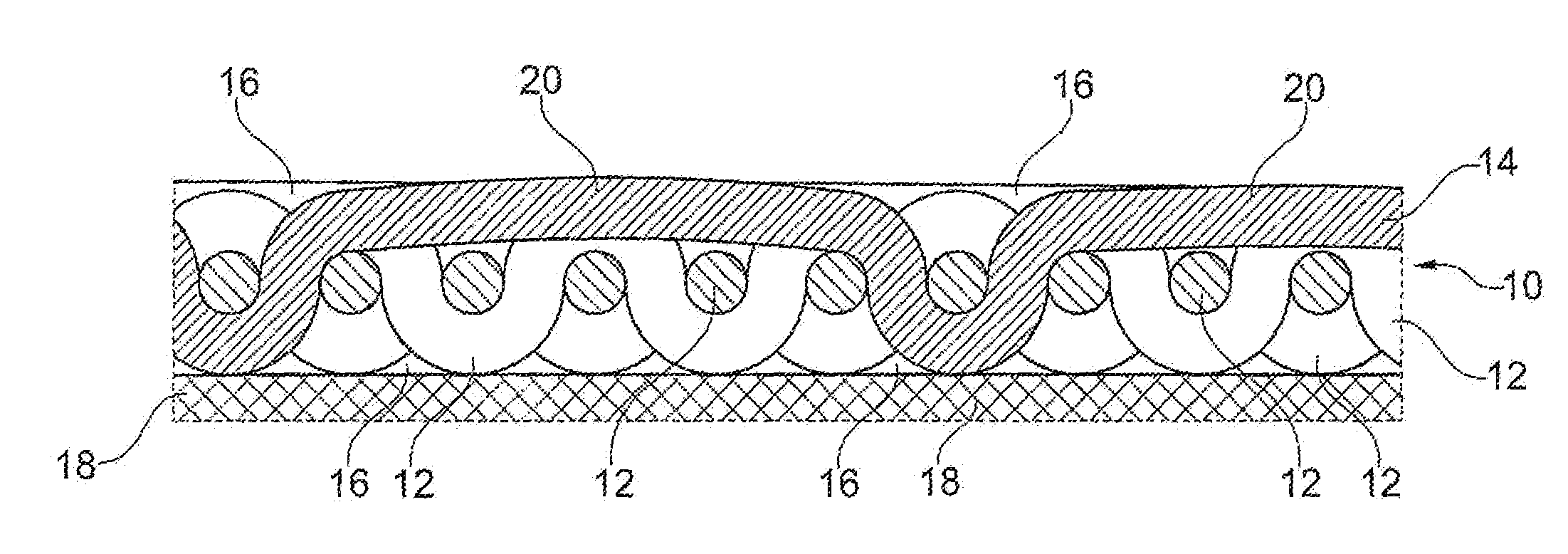
[0032]FIG. 1 shows a schematic cross-sectional view through the structure of an electrode substrate for an organic solar cell according to a first preferred embodiment. A fabric 10 shown in cross-section in FIG. 1 is made from PET filaments 12 having a thickness of 60 μm (more precisely: transparent PET filaments) with which metal fibres 14 (wires) composed of a CuAg alloy and having thickness of 60 μm are woven in the manner of a 5 / 1 twill weave, wherein metal wires 14 are each arranged parallel to and at a distance of 1 mm from each other, and extend only in the weft direction and, as shown in the cross-sectional view of FIG. 1, enclose five non-conductive fibres 12 extending transversely thereto, corresponding to a 5 / 1 twill weave.
[0033]This fabric structure is coated (filled or impregnated) with a resin layer (coating) 16 that comprises an ultraviolet-curing epoxy resin, and in the embodiment shown has been applied in the form of an indirect coating via transparent PET film 18 h...
PUM
| Property | Measurement | Unit |
|---|---|---|
| diameter | aaaaa | aaaaa |
| diameter | aaaaa | aaaaa |
| distance | aaaaa | aaaaa |
Abstract
Description
Claims
Application Information
 - R&D
- Intellectual Property
- Life Sciences
- Materials
- Tech Scout
- Unparalleled Data Quality
- Higher Quality Content
- 60% Fewer Hallucinations
Browse by: Latest US Patents, China's latest patents, Technical Efficacy Thesaurus, Application Domain, Technology Topic, Popular Technical Reports.
© 2025 PatSnap. All rights reserved.Legal|Privacy policy|Modern Slavery Act Transparency Statement|Sitemap|About US| Contact US: help@patsnap.com