Semiconductor device having ground shield structure and fabrication method thereof
a technology of ground shield structure and semiconductor device, which is applied in the direction of semiconductor device details, semiconductor/solid-state device details, inductance, etc., can solve the problems of large loss of silicon substrate at high frequencies, poor inductor performance, and affecting the performance of ic devices
- Summary
- Abstract
- Description
- Claims
- Application Information
AI Technical Summary
Benefits of technology
Problems solved by technology
Method used
Image

Examples
Embodiment Construction
[0024]Reference will now be made in detail to exemplary embodiments of the disclosure, which are illustrated in the accompanying drawings. Wherever possible, the same reference numbers will be used throughout the drawings to refer to the same or like parts.
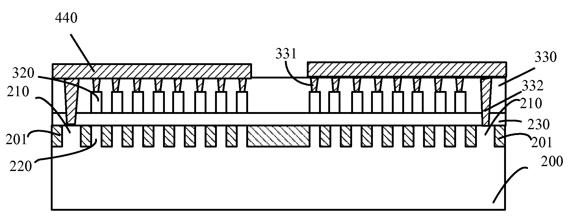
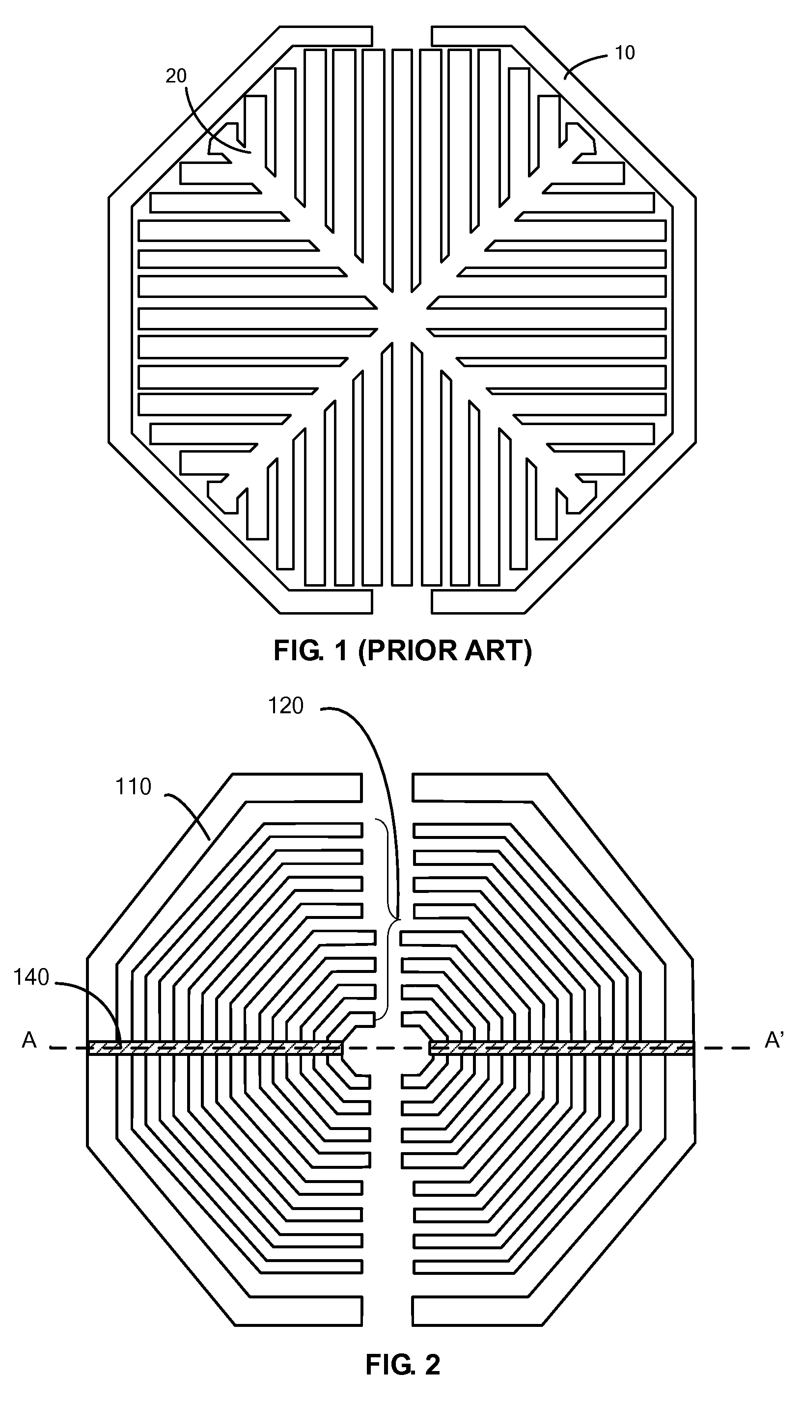
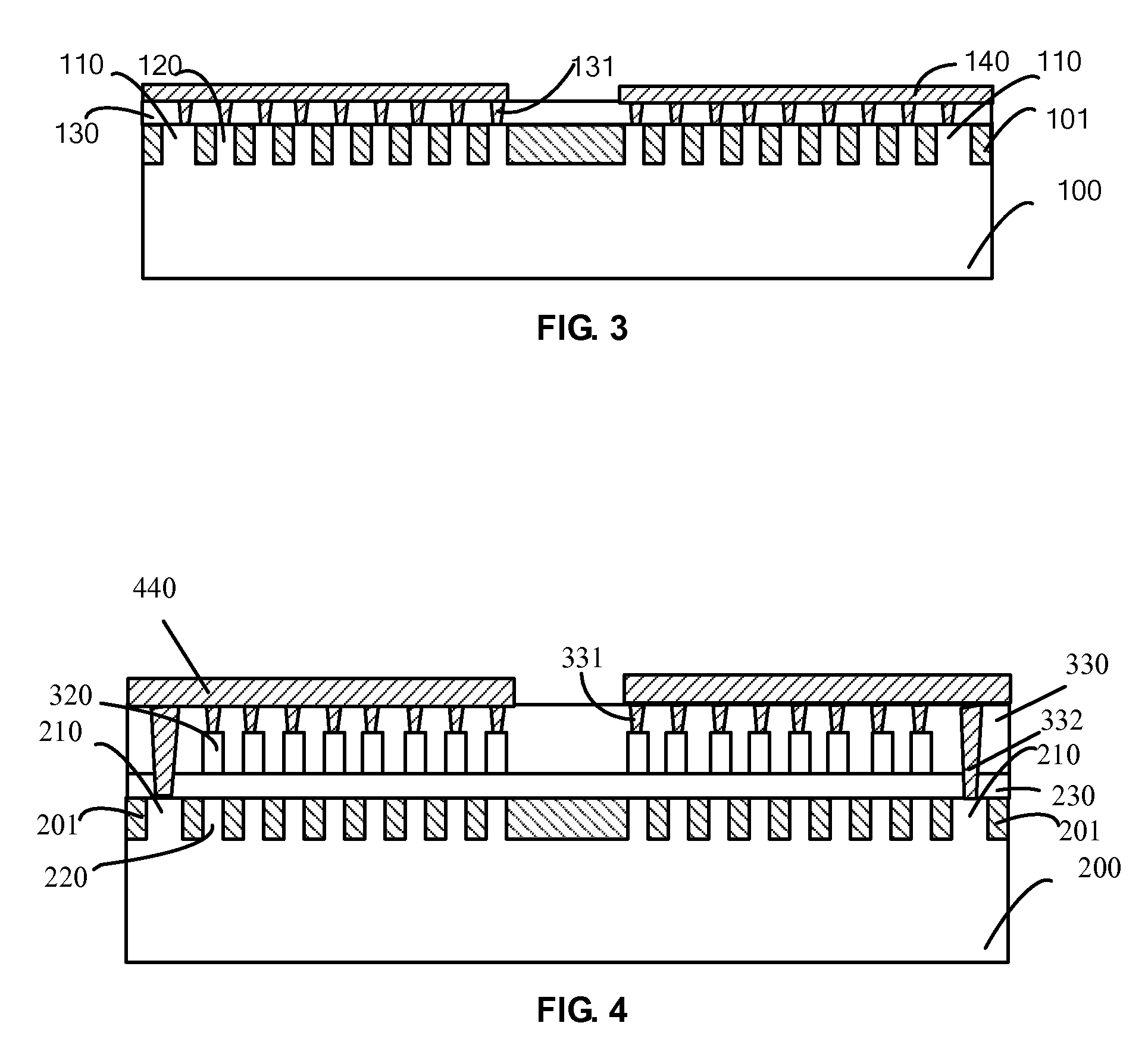
[0025]A ground shield may induce a large coupling capacitance at high frequencies and have a large contact area in the middle, which may generate large eddy current loss that reduces high quality factor (Q) of the inductor. As disclosed herein, semiconductor devices with ground shields are provided. The ground shield can be formed on a substrate, surrounded by a ground ring, and disposed under electronic device(s). An exemplary ground shield structure can include a plurality of coaxial conductive wirings (e.g., rings) and a metal wire passing in the radial direction through the conductive rings. Also, the metal wire can be connected to the ground ring. The ground shield fabricated in accordance with various disclosed embodiments c...
PUM
 Abstract
Description
Claims
Application Information
 - R&D
- Intellectual Property
- Life Sciences
- Materials
- Tech Scout
- Unparalleled Data Quality
- Higher Quality Content
- 60% Fewer Hallucinations
Browse by: Latest US Patents, China's latest patents, Technical Efficacy Thesaurus, Application Domain, Technology Topic, Popular Technical Reports.
© 2025 PatSnap. All rights reserved.Legal|Privacy policy|Modern Slavery Act Transparency Statement|Sitemap|About US| Contact US: help@patsnap.com