Low-latency thin film transistor, array substrate, and display panel

Inactive Publication Date: 2022-04-28
SHENZHEN CHINA STAR OPTOELECTRONICS SEMICON DISPLAY TECH CO LTD
View PDF1 Cites 0 Cited by
  • Summary
  • Abstract
  • Description
  • Claims
  • Application Information

AI Technical Summary

Benefits of technology

The present invention provides a thin film transistor, an array substrate, and a display panel with reduced latency and improved display performance. The technical effect of this invention is that at least part of the drain is located outside the region where the gate is located, which reduces the overlapping area between them and the coupling capacitance between them, which causes delay in a resistor-capacitor and impacts display performance.

Problems solved by technology

At present, in a structure of thin film transistors, an entire drain is disposed on a gate metal, and an overlapping area of the drain and the gate is large, resulting in a large coupling capacitance between the drain and the gate, which causes a large delay in a resistor-capacitor of a display panel, thereby affecting display performance of the display panel.
The present disclosure provide a low-latency thin film transistor, an array substrate, and a display panel to solve the problem that in a structure of current thin film transistors, the overlapping area of the drain and the gate is large, resulting in a large coupling capacitance between the drain and the gate, which causes a large delay in the resistor-capacitor of the display panel, thereby affecting display performance of the display panel.

Method used


Image

  • Low-latency thin film transistor, array substrate, and display panel
  • Low-latency thin film transistor, array substrate, and display panel
  • Low-latency thin film transistor, array substrate, and display panel

Examples


Embodiment Construction

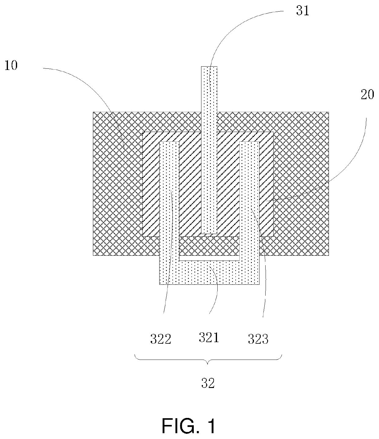
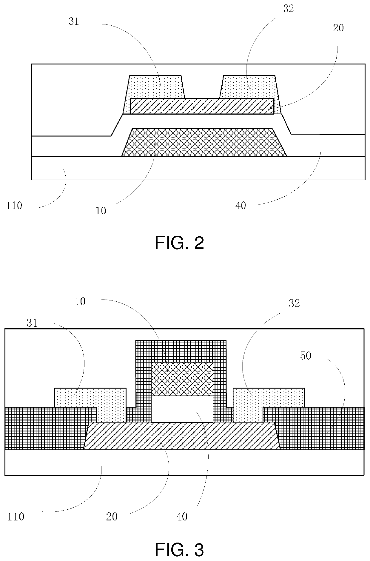
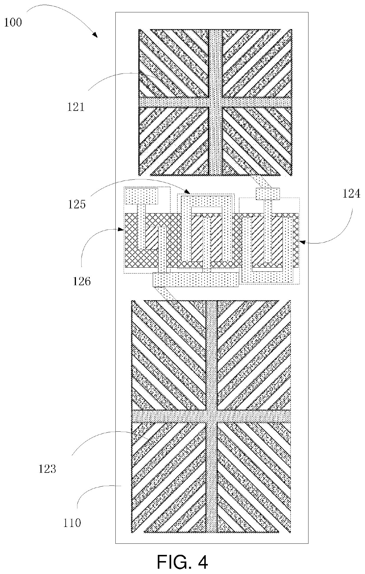
[0033]The following description of the embodiments with reference to the appended drawings is used for illustrating specific embodiments which may be used for carrying out the present disclosure. The directional terms described by the present disclosure, such as “upper”, “lower”, “front”, “back”, “left”, “right”, “inner”, “outer”, “side”, etc., are only directions by referring to the accompanying drawings. Thus, the adopted directional terms are used to describe and understand the present disclosure, but the present disclosure is not limited thereto. In figures, elements with similar structures are indicated by the same numbers.

[0034]In descriptions of the present disclosure, it should be noted that, orientations or position relationships indicated by the terms, such as “center”, “longitudinal”, “transverse”, “length”, “width”, “thickness”, “upper”, “lower”, “front”, “back”, “left”, “right”, “vertical”, “horizontal”, “top”, “bottom”, “inside”, “outside”, “clockwise”, “counterclockwi...


PUM


Abstract

The present invention provides a low-latency thin film transistor, an array substrate, and a display panel. The low-latency thin film transistor includes a gate, an active layer disposed on a side of the gate, and a source and a drain disposed above the gate, and the source and the drain are respectively connected to the active layer, wherein in a direction perpendicular to the active layer, at least part of an orthographic projection of the drain is located outside an orthographic projection of the gate.

Description

FIELD OF INVENTION[0001]The present disclosure relates to the field of display technology, and more particularly, to a low-latency thin film transistor, an array substrate, and a display panel.BACKGROUND OF INVENTION[0002]With development of display technology, in high refresh rate (such as 120 Hz) and high-resolution (such as 8K pixels) liquid crystal display panels, signal delay is a key factor restricting further development of the liquid crystal display panels. In thin film transistors (TFTs), a capacitance between a gate and a source / drain is directly affected by an overlapping area thereof.SUMMARY OF INVENTION[0003]At present, in a structure of thin film transistors, an entire drain is disposed on a gate metal, and an overlapping area of the drain and the gate is large, resulting in a large coupling capacitance between the drain and the gate, which causes a large delay in a resistor-capacitor of a display panel, thereby affecting display performance of the display panel.[0004]...

Claims


Application Information

Patent Timeline
IPC IPC(8): H01L27/12G02F1/1362
CPCH01L27/1251G02F1/136222H01L27/1218H01L27/1237H01L29/78618G02F1/1368H01L29/0847G02F1/13685G02F1/134345G02F1/13624H01L29/41733
Inventor LIN, MUNANPENG, BANGYINKIM, ILGON
Owner SHENZHEN CHINA STAR OPTOELECTRONICS SEMICON DISPLAY TECH CO LTD
Why Eureka
Try Eureka