
Gain control circuit, communication device, electronic appliance, and gain control method

a gain control circuit and communication device technology, applied in amplifiers, semiconductor devices/discharge tubes, amplifiers, etc., can solve problems such as intermodulation distortion, significant reduction of reception quality, and so on

Active Publication Date: 2015-11-10
SONY CORP
View PDF14 Cites 0 Cited by
  • Summary
  • Abstract
  • Description
  • Claims
  • Application Information

AI Technical Summary

Benefits of technology

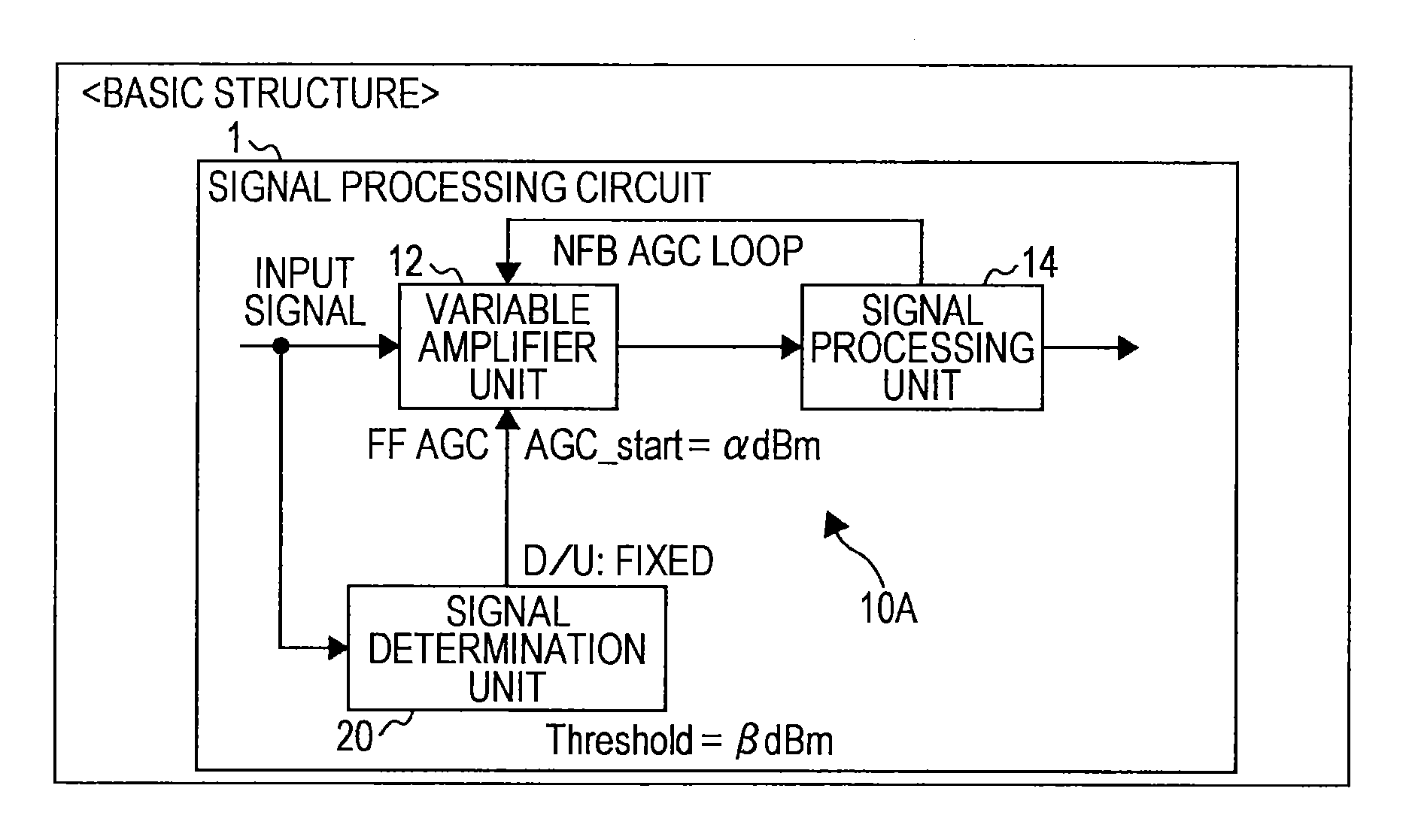
The gain control circuit, communication device, and electronic appliance described in this patent have a unique method for controlling the amplification factor of the first amplifier using feed forward. This results in a different gain control method than what was proposed in another Japanese patent. The technical effect of this patent is improved efficiency and accuracy in control over the amplification factor of the first amplifier in electronic devices.

Problems solved by technology

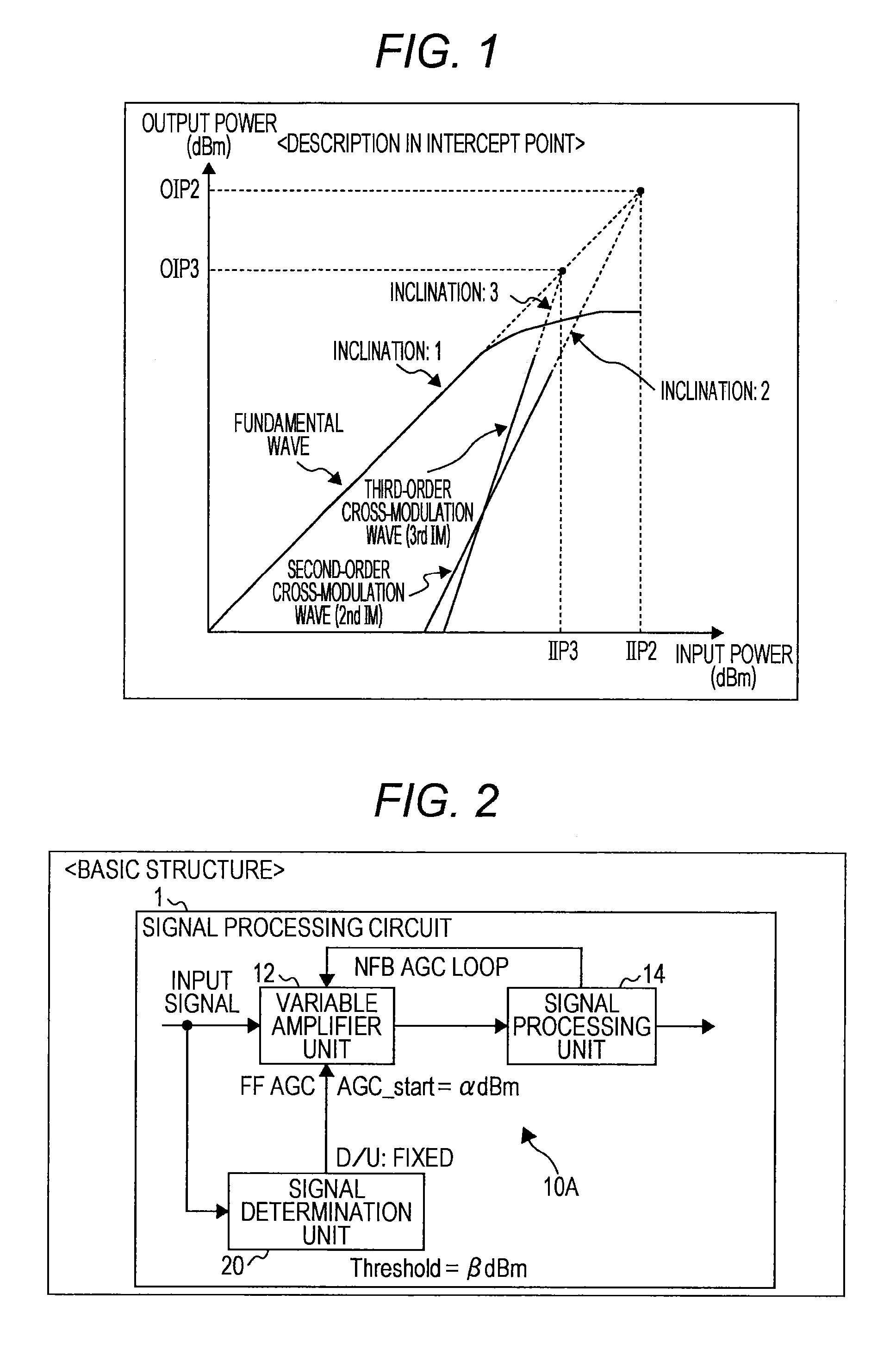
In an electronic circuit, in a case a plurality of signals at different frequencies are input, so-called intermodulation distortion arises a problem.
For example, in a case the difference of two carrier frequencies is present near the frequency of a desired wave, there is a problem of “intermodulation distortion” where an interfering component is also demodulated.
Typically, when signals at a plurality of frequencies adjacent to the receiving band of a self station are received, if the linear performance of an amplifier circuit or a frequency mixer circuit is poor, third-order distortion is caused within the receiving band (normally, only a first-order component of a modulated signal has to be taken into account), and the reception quality is significantly reduced.
However, this method increases the cost regarding the bandpass filter, or increases the size of the substrate, for example.
Also, since generally the bandpass filter acts only with respect to a fixed frequency, using the same while making the corresponding frequency variable is difficult, and the bandpass filter has to be prepared for each communication channel (in other words, a carrier frequency; hereinafter also referred to as a “band”).
For example, to improve the linear performance of a circuit, a measure of increasing the bias current or optimizing the DC bias point such that operation is in a linear region as much as possible is effective, but this increases the power supply voltage or increases the consumption power.
Or, it is also conceivable to use an expensive circuit member with improved linearity, but even if an expensive circuit member is used, the non-linearity cannot, in principle, be made zero.
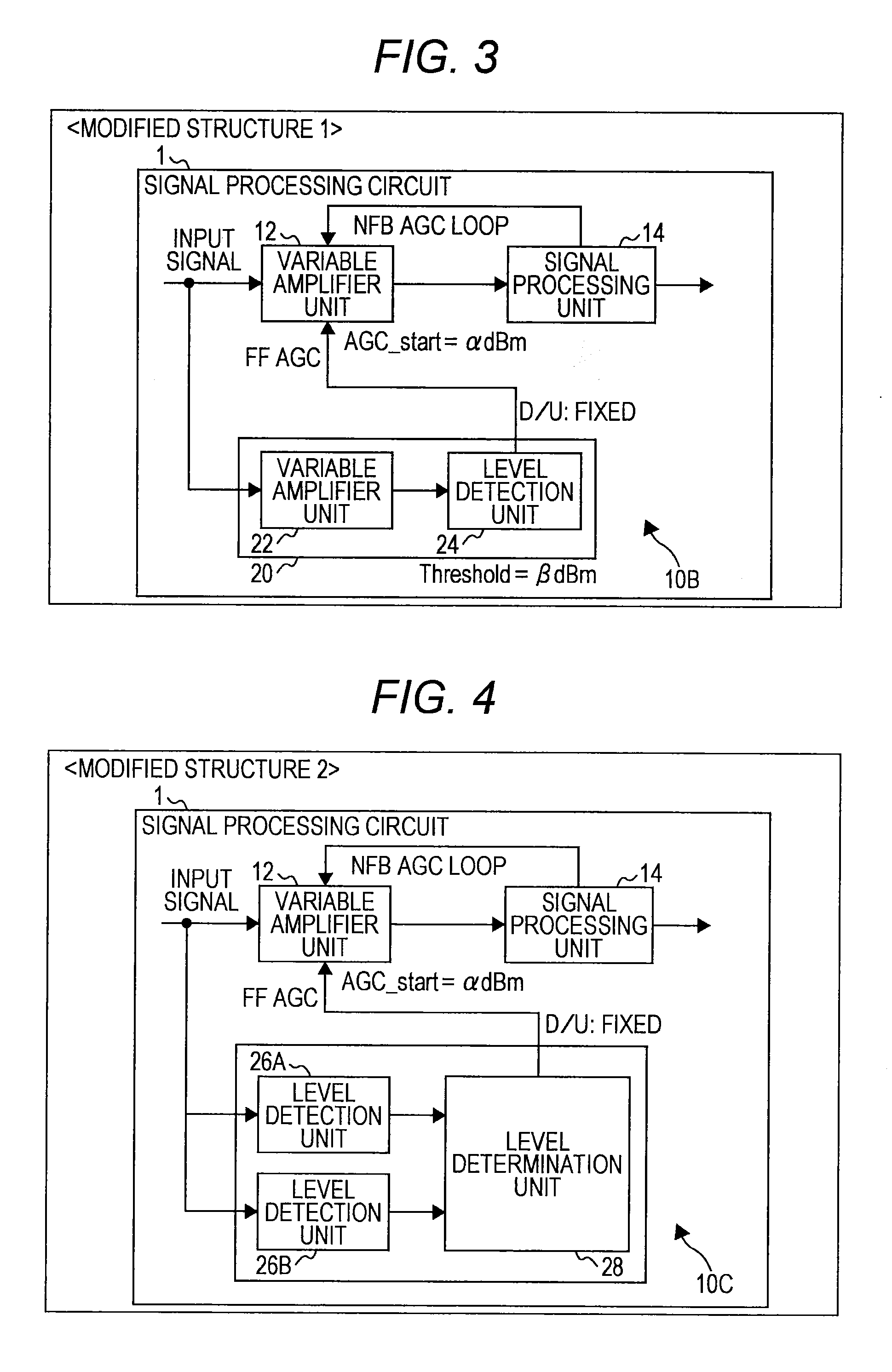
However, the technology proposed in Japanese Patent Application Laid-Open No. 2000-244353 includes two stages of gain control circuits in a system for input signals, and includes a level detection circuit (a wave detector) for each gain control circuit, and thus, the circuit is complicated.

Method used


Image

  • Gain control circuit, communication device, electronic appliance, and gain control method
  • Gain control circuit, communication device, electronic appliance, and gain control method
  • Gain control circuit, communication device, electronic appliance, and gain control method

Examples


example 1

Operation of Example 1

[0088]FIGS. 7 to 9 are diagrams for describing an operation of the communication device 810A of Example 1. Here, FIG. 7 is a diagram showing a relationship between an input level and an SN ratio (SNR) of the communication device 810A. FIG. 8 is a diagram showing a relationship between the amount of attenuation of the input amplifier unit 812 and an SN ratio and IIP3 where a desired wave is at −30 dBm. FIG. 9 is a diagram showing a relationship between the amount of attenuation of the input amplifier unit 812 and an SN ratio and IIP3 where a desired wave is at −14 dBm.

[0089]As shown in FIG. 7, the start point of AGC is at −50 dBm. It can be seen that the noise characteristic is desirable when the input level is high.

[0090]FIG. 8 shows operating points where the desired wave is at −30 dBm, and at this time, the threshold of the level detection unit 824 is set at −30 dBm. For example, when assuming the required IIP3 where the signal level of an interfering wave is...

example 2

Structure

[0092]FIG. 10 is a diagram for describing a communication device (including a receiving circuit) of Example 2. A communication device 810B is different from the communication device 810A of Example 1 in the structure of the signal determination unit 820. Specifically, a signal determination unit 820B includes a variable amplifier unit 822 (corresponding to the variable amplifier unit 22), and a level detection unit 824 (corresponding to the level detection unit 24). As the variable amplifier unit 822, a wide bandwidth variable gain amplifier is used so that the interfering wave can also be appropriately processed, but since the noise characteristic does not have to be good, one which is proportionally smaller in size than the variable amplifier unit 812 on the main signal path is used. The signal determination unit 820B is provided before the input amplifier unit 812, and the detection result is used as the gain control signal GC2, and the input amplifier unit 812 is thereb...

example 3

[0101]FIG. 12 is a diagram for describing Example 3. Here, (A) of FIG. 12 shows an arrangement image of a plurality of communication devices within an electronic appliance, (B) of FIG. 12 shows an example detailed structure of the communication devices, and (C) of FIG. 12 shows an example of frequency arrangement of carrier frequencies.

[0102]Example 3 is an example application where a plurality of communication devices are arranged inside the housing of one electronic appliance and communication is performed. For example, this is a mode where all the communication devices (communication chips) are mounted on the same board in one electronic appliance, and each carrier carrier frequency is set in advance. A case is assumed where more than three sets regarding transmission / reception are randomly arranged on the circuit board inside the electronic appliance with no respect to the arrangement, the directivity of the radio wave or the like.

[0103]For example, in FIG. 12, a case where 3-ba...


PUM


Abstract

The present technology relates to a gain control circuit, a communication device, an electronic appliance, and a gain control method which aim to provide a technology capable of suppressing intermodulation distortion. The gain control circuit includes a first amplifier for amplifying an input signal, and a signal determination unit for determining an input signal to be input to the first amplifier, and controlling an amplification factor of the first amplifier based on the determination result. The communication device includes a first amplifier for amplifying a received signal, a receiving unit for performing a receiving process based on a signal output from the first amplifier, and a signal determination unit for determining a received signal to be input to the first amplifier, and controlling the amplification factor of the first amplifier based on the determination result. In the gain control method, an input signal to be input to a first amplifier for amplifying an input signal is determined, and the amplification factor of the first amplifier is controlled by a feed forward system based on the determination result.

Description

TECHNICAL FIELD[0001]The technology disclosed in the present specification relates to a gain control circuit, a communication device, an electronic appliance, and a gain control method.BACKGROUND ART[0002]In an electronic circuit, in a case a plurality of signals at different frequencies are input, so-called intermodulation distortion arises a problem. For example, a case of an amplifier circuit provided at an input stage of a receiving circuit is typical. For example, in a case the difference of two carrier frequencies is present near the frequency of a desired wave, there is a problem of “intermodulation distortion” where an interfering component is also demodulated. Typically, when signals at a plurality of frequencies adjacent to the receiving band of a self station are received, if the linear performance of an amplifier circuit or a frequency mixer circuit is poor, third-order distortion is caused within the receiving band (normally, only a first-order component of a modulated ...

Claims


Application Information

Patent Timeline
Patent Type & Authority Patents(United States)
IPC IPC(8): H04B1/06H04B7/00H03G3/30
CPCH03G3/3042H03G3/3052H03G3/3068
Inventor TAKAHASHI, KATSUAKIYOSHIKAWA, NAOTO
Owner SONY CORP
Learn More