Method for fabricating memory device
- Summary
- Abstract
- Description
- Claims
- Application Information
AI Technical Summary
Benefits of technology
Problems solved by technology
Method used
Image

Examples
Embodiment Construction
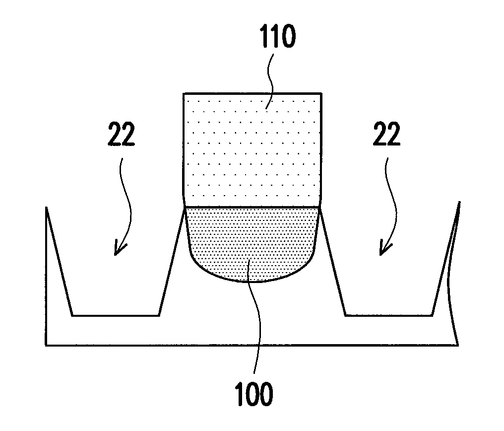
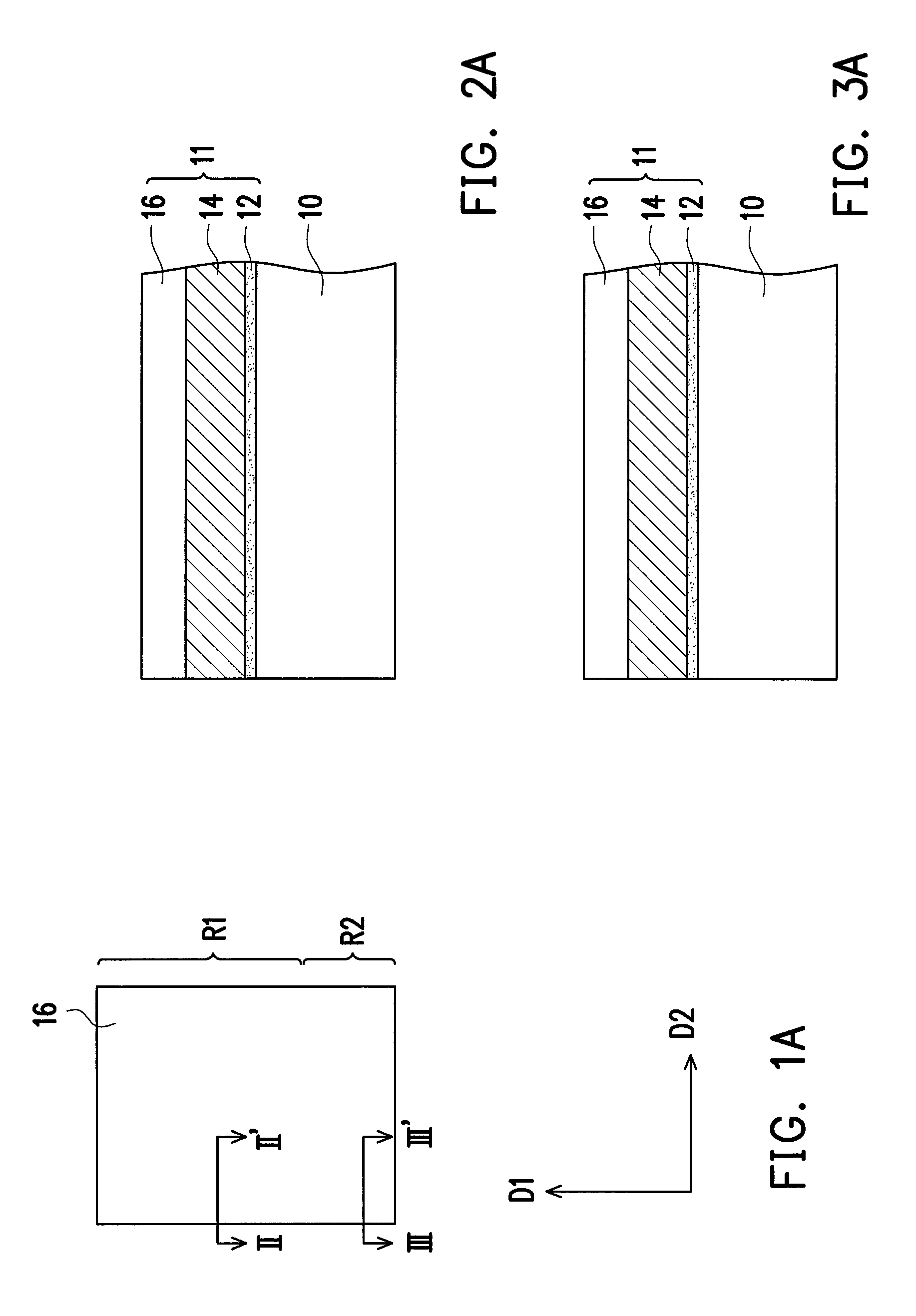
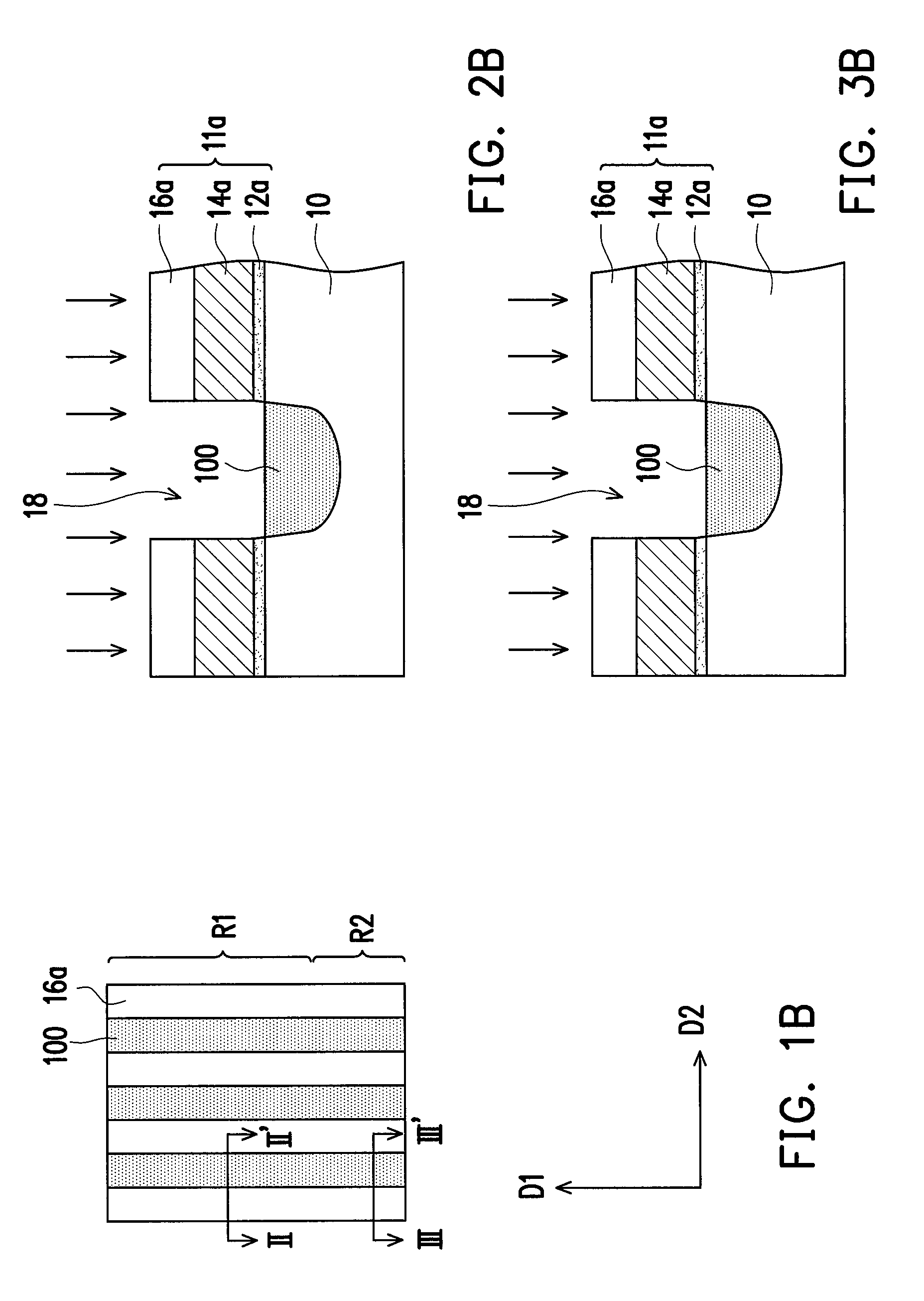
[0031]FIGS. 1A to 1K are top views illustrating a flow for fabricating a memory device according to an embodiment of the invention. FIGS. 2A to 2K are respectively cross-sectional schematic views taken along a II-II′ line in FIGS. 1A to 1K. FIGS. 3A to 3K are respectively cross-sectional schematic views taken along a III-III′ line in FIGS. 1A to 1K. FIG. 4 is a cross-sectional schematic view taken along a IV-IV′ line in FIG. 1K.
[0032]Referring to FIGS. 1A, 2A, and 3A, first of all, a stack layer 11 is formed on a substrate 10. The substrate 10 has a first region R1 and a second region R2, as shown in FIG. 1A. In an embodiment of the invention, the first region R1 may be an active region, for example, while the second region R2 may be a peripheral region, for example. The substrate 10 is a semiconductor substrate, a semiconductor compound substrate, or a semiconductor-over-insulator (SOI) substrate. The semiconductor is, for example, atoms in group IVA, such as silicon or germanium. ...
PUM
 Abstract
Description
Claims
Application Information
 - R&D
- Intellectual Property
- Life Sciences
- Materials
- Tech Scout
- Unparalleled Data Quality
- Higher Quality Content
- 60% Fewer Hallucinations
Browse by: Latest US Patents, China's latest patents, Technical Efficacy Thesaurus, Application Domain, Technology Topic, Popular Technical Reports.
© 2025 PatSnap. All rights reserved.Legal|Privacy policy|Modern Slavery Act Transparency Statement|Sitemap|About US| Contact US: help@patsnap.com