
Cu—Ni—Si alloy for electronic material

a technology of electronic materials and alloys, applied in the field of precipitation hardened copper alloys, can solve the problems of difficult control of particle size and density, insufficient favorable influence on strength, and difficulty in precipitating small particles, and achieve the effect of increasing the characteristics of corson alloys

Active Publication Date: 2015-04-14
JX NIPPON MINING & METALS CORP
View PDF24 Cites 2 Cited by
  • Summary
  • Abstract
  • Description
  • Claims
  • Application Information

AI Technical Summary

Benefits of technology

The inventors conducted research to find a solution for improving the strength and electrical conductivity of Corson alloy. They discovered that by controlling the sizes and number densities of two types of Ni—Si compound particles, they could create a balance between strength and electrical conductivity. Small particles of 0.01 to 0.3 μm size and 1 to 2000 / μm2 number density are controlled to enhance the alloy's strength, while large particles of 0.3 to 1.5 μm size and 0.05 to 2 / μm2 number density are controlled to enhance its electrical conductivity. This results in a Corson alloy with improved characteristics.

Problems solved by technology

In addition Japanese Patent No. 3797736 describes the respective precipitation of large particles and small particles by perforating aging twice, but it is difficult to precipitate the small particles in a second aging since the concentration of Ni and Si to be solid-solubilized is lower than that of the particles in a first aging, and favorable influence on strength is insufficient since the number density and the particle size are small (see Comparative Example 5 described below).
A technique of performing aging twice has a problem in that controlling the particle size and the density is difficult since the amount of Ni and Si to be solid-solubilized changes depending on the first aging.
These large particles become coarse depending on the amount of additive elements or the temperature condition, and it is likely to exert adverse influence on bending workability.

Method used


Image

  • Cu—Ni—Si alloy for electronic material
  • Cu—Ni—Si alloy for electronic material

Examples


example

[0081]Hereinafter, specific examples of the invention will be described, but these examples are provided to help better understanding of the invention and its advantages, and are not intended to limit the invention by any means.

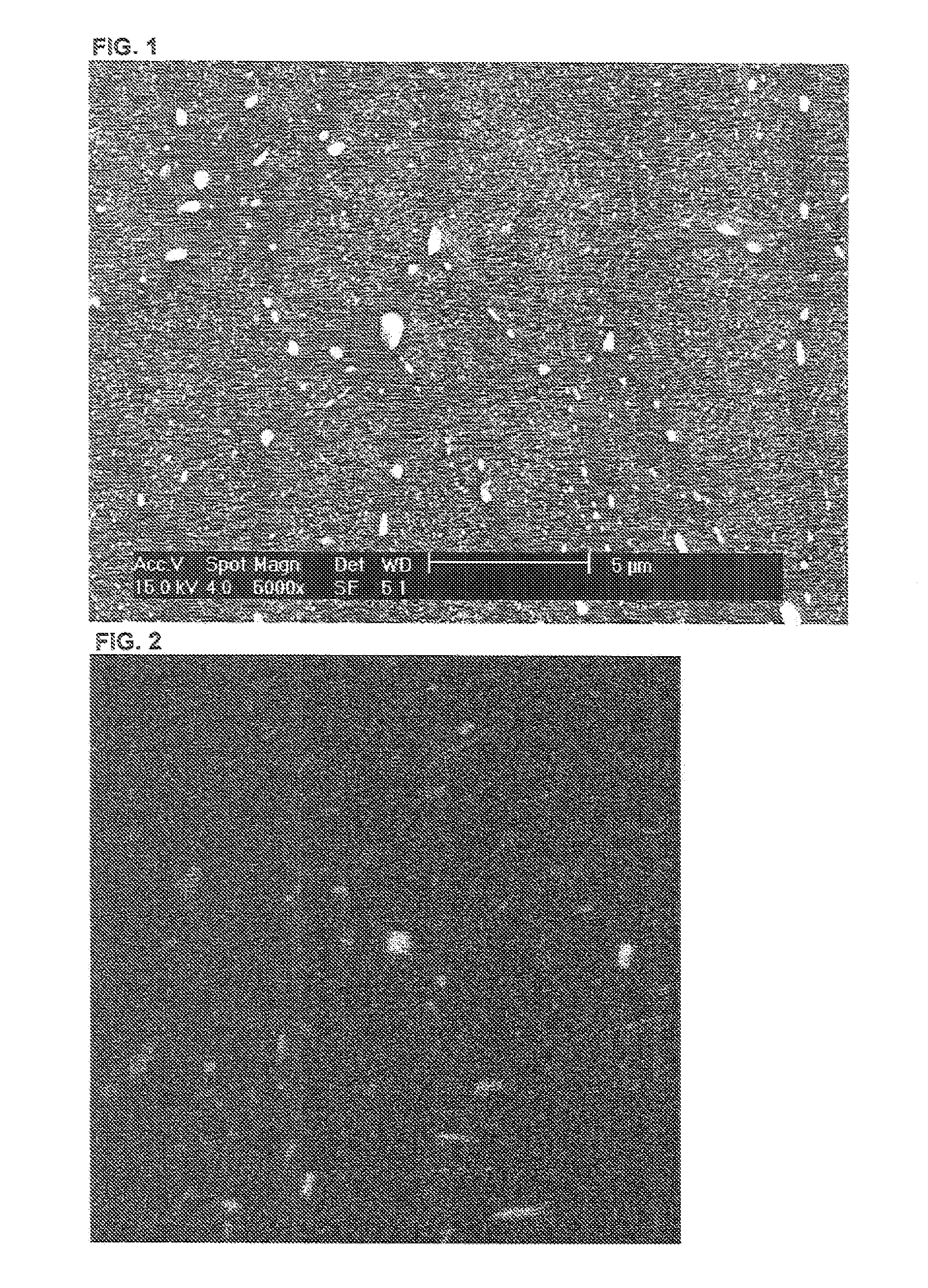
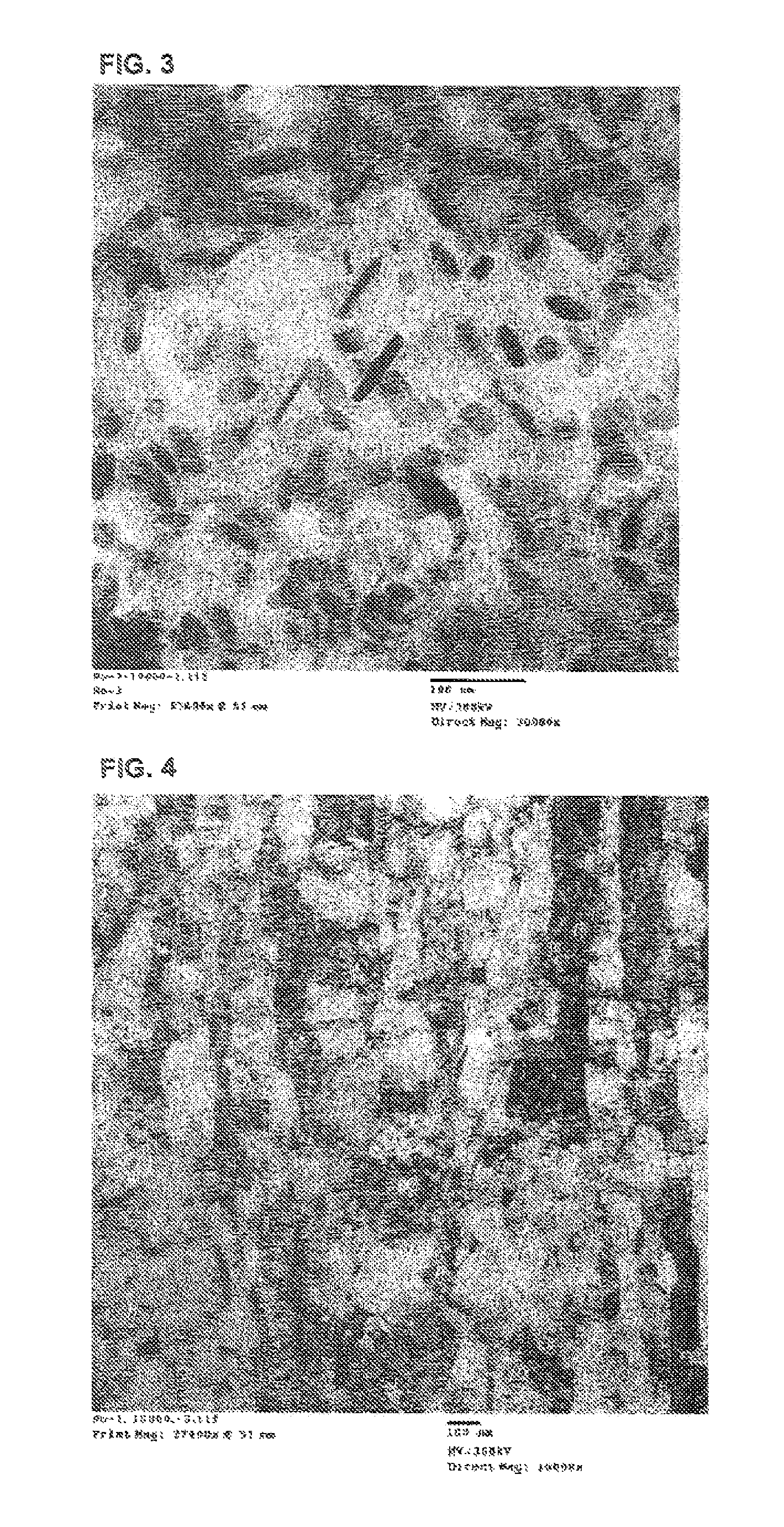
[0082]Copper alloys with various component compositions indicated in Tables 1 to 4 were melted in a high frequency melting furnace, were maintained at each melting holding temperature, and were cast into an ingot having a thickness of 30 mm. Thereafter, this ingot was heated at each reheating treatment temperature, then was hot rolled at 850 to 1050° C. for 0.5 to 5 hours (the material temperature at the time of completion of hot rolling was 500° C.) to obtain a plate thickness of 10 mm, and then surface grinding was applied by a thickness of 8 mm in order to remove scale at the surface. Subsequently, after the plate thickness becomes 0.15 mm or 0.10 mm by the cold rolling, solution treatment was earned out under the conditions indicated in Tables 1 to 4. Sub...


PUM

PropertyMeasurementUnit
particle sizeaaaaaaaaaa

Abstract

The distribution of Ni—Si compound grains is controlled to thereby improve the properties of Corson alloys. The copper alloy for electronic materials comprises 0.4 to 6.0% mass of Ni and 0.1 to 1.4% by mass of Si, with the balance being Cu and unavoidable impurities.The copper alloy comprising:small particles of Ni—Si compound having a particle size of equal to or greater than 0.01 μm and smaller than 0.3 μm; andlarge particles of Ni—Si compound having a particle size of equal to of greater than 0.3 μm and smaller than 1.5 μm.The number density of the small particles is 1 to 2000 pieces / μm2 and the number density of the large particles is 0.05 to 2 pieces / μm2.

Description

BACKGROUND OF THE INVENTION[0001]1. Field of the Invention[0002]The present invention relates to a precipitation hardened copper alloy, and more particularly, to a Cu—Ni—Si alloy suitable for the use in various components of electronic equipment.[0003]2. Description of the Related Art[0004]Copper alloys for electronic materials used in various components of electronic equipment such as lead frames, connectors, pins, terminals, relays, and switches are required to achieve a balance between high strength and high electrical conductivity (or thermal conductivity) as basic characteristics. In recent years, high integration, miniaturization and thickness reduction of electronic components are in rapid progress, and in this respect, a demand for a copper alloy to be used in the components of electronic equipment is rising to higher levels.[0005]From the viewpoints of high strength and high electrical conductivity, the amount of use of precipitation hardened copper alloys is increasing in ...

Claims


Application Information

Patent Timeline
Patent Type & Authority Patents(United States)
IPC IPC(8): C22C9/06C22C9/10C22C1/10C22F1/00C22F1/08
CPCC22C9/06C22F1/08C22C1/10C22F1/00C22C9/00
Inventor OOKUBO, MITSUHIRO
Owner JX NIPPON MINING & METALS CORP
Learn More