Semiconductor device
a technology of semiconductors and semiconductors, applied in the direction of semiconductor devices, electrical equipment, transistors, etc., can solve the problems of deterioration achieve the effects of suppressing the change of the electrical characteristics of the transistor, high resistance to chemical liquid, and high barrier property against impurities
- Summary
- Abstract
- Description
- Claims
- Application Information
AI Technical Summary
Benefits of technology
Problems solved by technology
Method used
Image
Examples
embodiment 1
[Embodiment 1]
[0090]In this embodiment, a transistor of one embodiment of the present invention will be described.
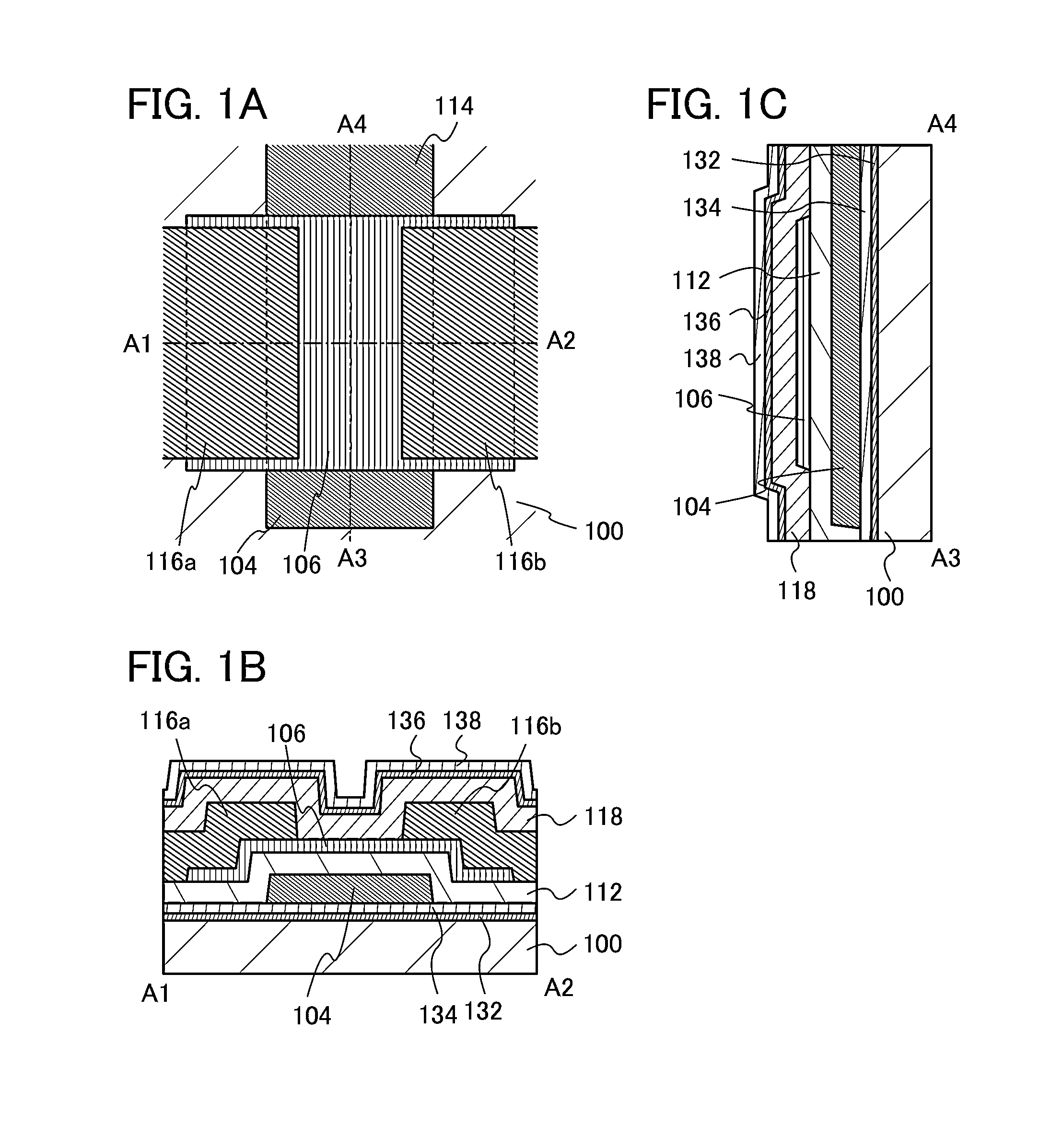
[0091]FIG. 1A is a top view of a transistor of one embodiment of the present invention. FIG. 1B is a cross-sectional view taken along dashed-dotted line A1-A2 in FIG. 1A. FIG. 1C is a cross-sectional view taken along dashed-dotted line A3-A4 in FIG. 1A. Note that for simplicity, a gate insulating film 112 and the like are not illustrated in FIG. 1A.
[0092]FIG. 1B is a cross-sectional view of a transistor including a crystalline insulating film 132 over a substrate 100; an aluminum oxide film 134 over the crystalline insulating film 132; a gate electrode 104 over the aluminum oxide film 134; the gate insulating film 112 over the gate electrode 104; a semiconductor film 106 which is over the gate insulating film 112 and overlaps with the gate electrode 104; a source electrode 116a and a drain electrode 116b over the semiconductor film 106; a crystalline insulating film 136 ...
embodiment 2
[Embodiment 2]
[0271]In this embodiment, methods for manufacturing the transistors described in Embodiment 1 will be described.
[0272]First, a method for manufacturing the transistor illustrated in FIGS. 1A to 1C will be described with reference to FIGS. 7A to 7D and FIGS. 8A to 8C. Note that only cross-sectional views corresponding to FIG. 1B are shown for simplicity in FIGS. 7A to 7D and FIGS. 8A to 8C.
[0273]First, the substrate 100 is prepared. As the substrate 100, a substrate selected from the substrates given as examples of the substrate 100 can be used.
[0274]Next, the crystalline insulating film 132 is formed (see FIG. 7A). The crystalline insulating film 132 can be formed using an insulating film selected from the insulating films given as examples of the crystalline insulating film 132 and can be formed by a sputtering method, a chemical vapor deposition (CVD) method, a molecular beam epitaxy (MBE) method, an atomic layer deposition (ALD) method, or a pulsed laser deposition ...
embodiment 3
[Embodiment 3]
[0437]In this embodiment, a transistor of one embodiment of the present invention will be described.
[0438]FIG. 20A is a top view of a transistor of one embodiment of the present invention. FIG. 20B is a cross-sectional view taken along dashed-dotted line G1-G2 in FIG. 20A. FIG. 20C is a cross-sectional view taken along dashed-dotted line G3-G4 in FIG. 20A. Note that for simplicity, a gate insulating film 2112 and the like are not illustrated in FIG. 20A.
[0439]FIG. 20B is a cross-sectional view of a transistor including a gate electrode 2104 over a substrate 2100; the gate insulating film 2112 over the gate electrode 2104; a semiconductor film 2106 which is over the gate insulating film 2112 and overlaps with the gate electrode 2104; a source electrode 2116a and a drain electrode 2116b over the semiconductor film 2106; and a protective insulating film 2118 over the semiconductor film 2106, and the source electrode 2116a and the drain electrode 2116b. Note that the gate ...
PUM
 Abstract
Description
Claims
Application Information
 - R&D
- Intellectual Property
- Life Sciences
- Materials
- Tech Scout
- Unparalleled Data Quality
- Higher Quality Content
- 60% Fewer Hallucinations
Browse by: Latest US Patents, China's latest patents, Technical Efficacy Thesaurus, Application Domain, Technology Topic, Popular Technical Reports.
© 2025 PatSnap. All rights reserved.Legal|Privacy policy|Modern Slavery Act Transparency Statement|Sitemap|About US| Contact US: help@patsnap.com


