
Light-emitting device and manufacturing method thereof

a technology of light-emitting devices and manufacturing methods, which is applied in the manufacture of final products, electric discharge tubes/lamps, sustainable manufacturing/processing, etc., can solve the problems of low hermeticity and difficulty in using such sealing methods, and achieve high flexibility, high reliability, and high reliability.

Inactive Publication Date: 2015-01-06
SEMICON ENERGY LAB CO LTD
View PDF11 Cites 11 Cited by
  • Summary
  • Abstract
  • Description
  • Claims
  • Application Information

AI Technical Summary

Benefits of technology

[0019]In view of the above, an object of one embodiment of the present invention is to provide a light-emitting device which is thin and lightweight and has high flexibility, impact resistance, and reliability. Another object of one embodiment of the present invention is to provide a light-emitting device which is thin and lightweight and has high flexibility, impact resistance, and hermeticity.
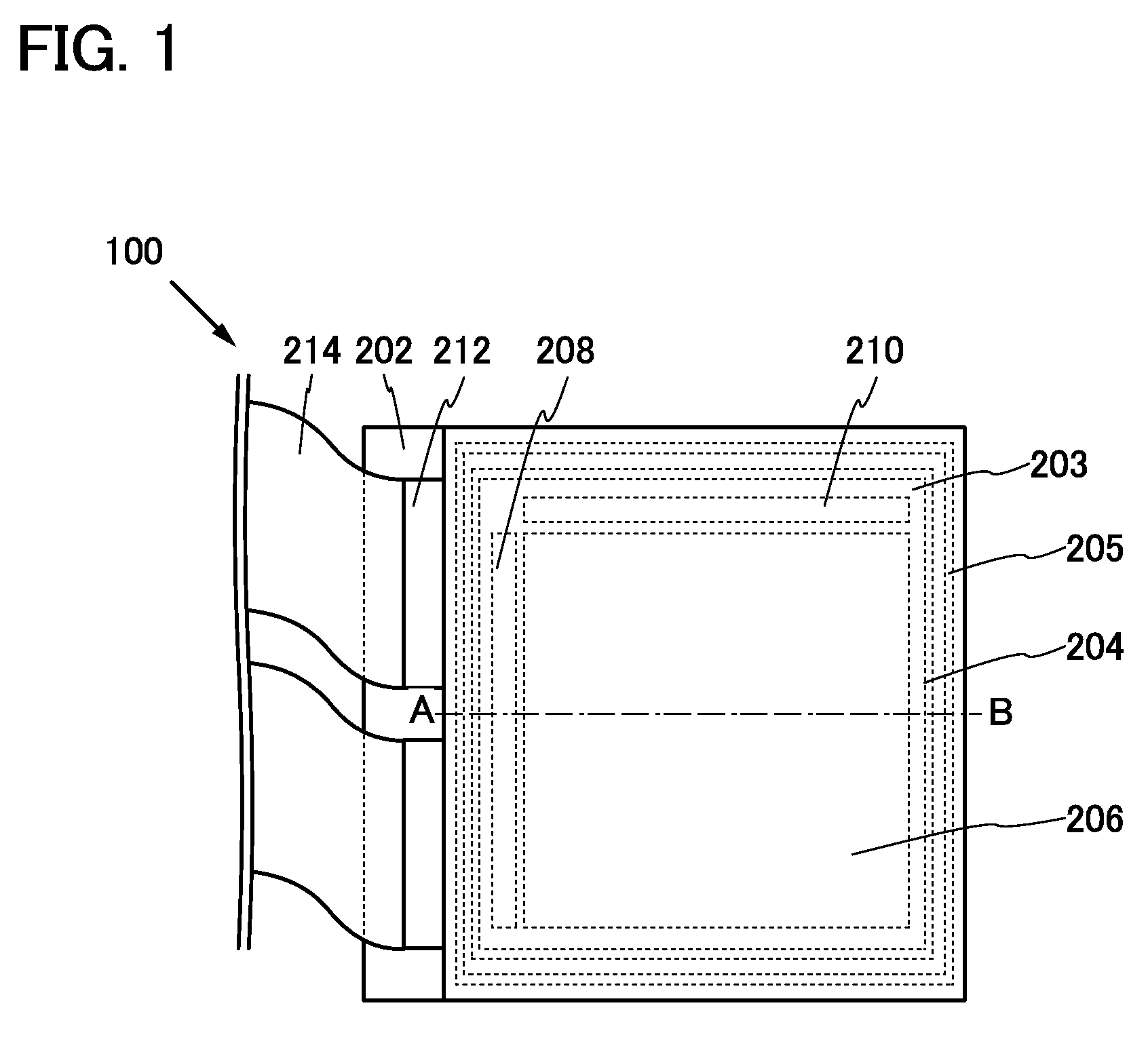
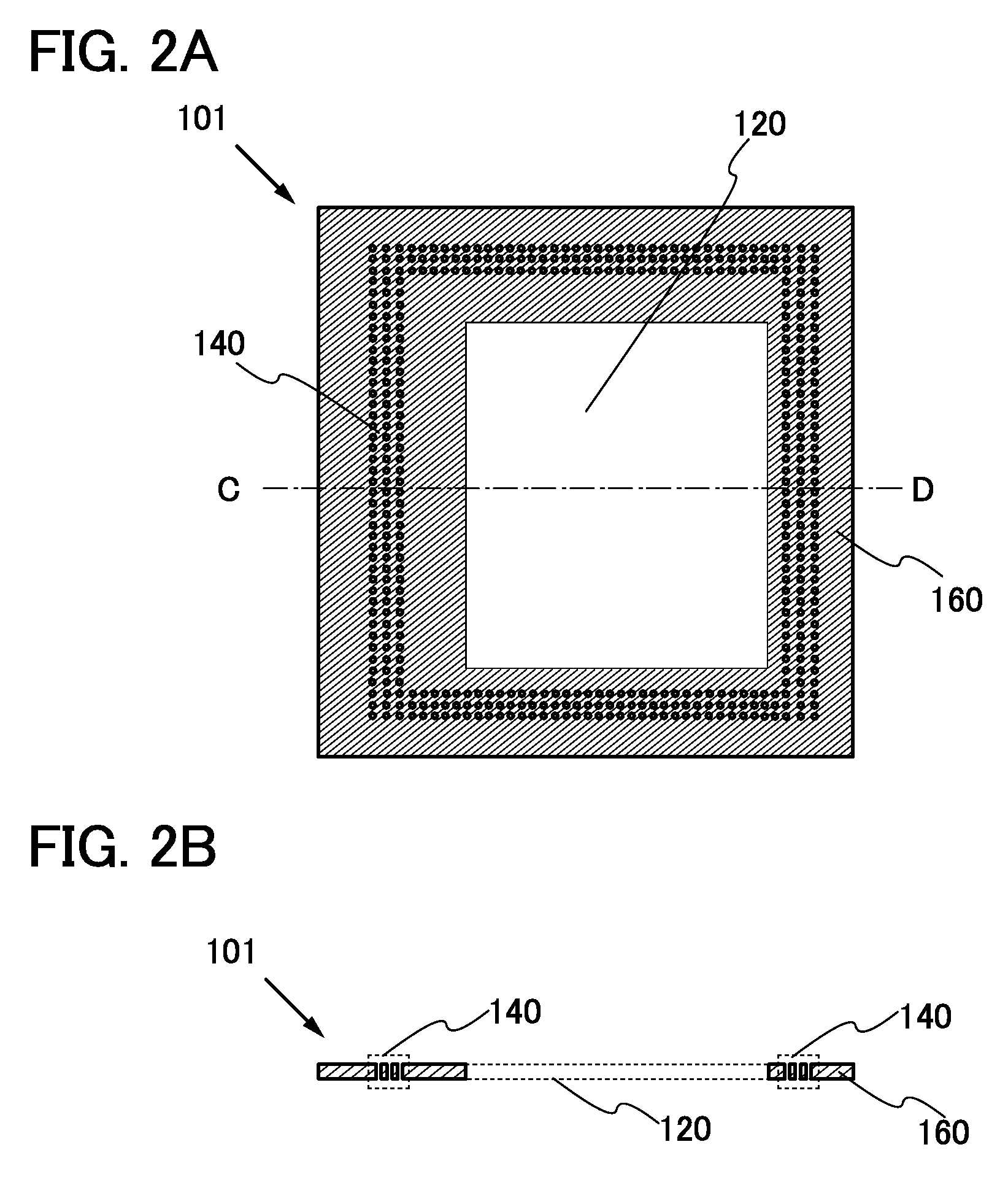
[0025]The second flexible substrate includes the openings (second openings) at a position where the frit glass is provided, specifically around the region facing the light-emitting region (i.e., around the first opening). The openings (second openings) are filled with the frit glass. The frit glass is provided on both sides of the second flexible substrate through the openings (second openings), whereby adhesion strength between the second flexible substrate and the frit glass can be increased. Accordingly, hermeticity of the light-emitting device can be further increased.
[0031]In the manufacturing method, the second flexible substrate can be provided over the supporting base with a space interposed therebetween and frit glass can be formed in the space. Thus, the openings (second openings) around the region overlapping with the light-emitting region are filled with the frit glass, so that the light-emitting device in which the frit glass is provided around the openings (second openings) on both surfaces of the second flexible substrate can be manufactured.
[0037]In the above manufacturing method, since the adhesive layer is formed of the organic resin and has a possibility of transmitting atmospheric components (including moisture and oxygen) more than a little, an inorganic insulating layer which is in contact with the second flexible substrate and covers the adhesive layer and the coloring layer is formed, which makes it possible to suppress the entry of the atmospheric components from the adhesive layer. Accordingly, a light-emitting device with high reliability can be manufactured.
[0038]According to one embodiment of the present invention, a light-emitting device which is thin and lightweight and has high flexibility, impact resistance, and reliability can be provided. Further, a light-emitting device which is thin and lightweight and has high flexibility, impact resistance, and hermeticity can be provided.

Problems solved by technology

When the baking of the frit paste is insufficient, the binder or the like might remain in the frit glass which has been irradiated with the laser light, resulting in low hermeticity, or a crack might be generated in the frit glass to break the sealing.
Thus, it is difficult to use such a sealing method using frit glass as a method for forming a sealed body.

Method used


Image

  • Light-emitting device and manufacturing method thereof
  • Light-emitting device and manufacturing method thereof
  • Light-emitting device and manufacturing method thereof

Examples


embodiment 1

[0057]In this embodiment, a light-emitting device which is one embodiment of the present invention and a method for manufacturing the light-emitting device are described. In this embodiment, a display device including a light-emitting element as a light-emitting device and a method for manufacturing the display device are described.

[0058]A display device which is one embodiment of the present invention includes a layer including at least a transistor and a light-emitting element between a first flexible substrate and a second flexible substrate each of which has an insulating surface. The first flexible substrate is bonded to the second flexible substrate with frit glass containing low-melting glass.

[0059]The first flexible substrate is provided with the layer including a transistor and a light-emitting element. The second flexible substrate is provided on the side to which light from the light-emitting element is emitted. Thus, light can be extracted from the second flexible substr...

embodiment 2

[0179]In this embodiment, as a method for manufacturing the light-emitting device which is one embodiment of the present invention, a method which is partly different from the manufacturing method in the above embodiment is described. Note that also in this embodiment, the display device 100 is exemplified.

[0180]The manufacturing method described in this embodiment is different from the manufacturing method described in Embodiment 1 in that frit glass is also formed over the first flexible substrate 202 (specifically, an insulating layer included in a transistor in the layer 220 including the transistor and a light-emitting element).

[0181]First, the separation layer 252, the first flexible substrate 202, the insulating layer 218, and a transistor are formed over the supporting base 250. Frit glass 276 is formed over an insulating layer included in the transistor and then a light-emitting element is formed to be in contact with the transistor, whereby the layer 220 including a transi...

embodiment 3

[0188]In this embodiment, as a light-emitting device of one embodiment of the present invention, a light-emitting device which is partly different from the light-emitting device described in the above embodiment is described. Further, a method for manufacturing the light-emitting device is described. Note that also in this embodiment, the display device 100 is exemplified.

[0189]The display device described in this embodiment is different from the display device 100 in that a spacer is provided between an element substrate and a counter substrate (see FIG. 11A).

[0190]The display device described in this embodiment includes a spacer 278 which is in contact with the layer 220 including a transistor and a light-emitting element and the insulating layer 236. In particular, the spacer 278 is preferably provided in a position overlapping with the light-blocking layer 234. Although not shown in FIGS. 11A and 11B, the spacer 278 may be provided over a partition which covers the outer region ...


PUM


Abstract

A light-emitting device which is thin and lightweight and has high flexibility, impact resistance, and reliability is provided. Further, a light-emitting device which is thin and lightweight and has high flexibility, impact resistance, and hermeticity is provided. In the light-emitting device in which a light-emitting region including a transistor and a light-emitting element is sealed between a first flexible substrate and a second flexible substrate, an opening is provided in the second flexible substrate around a region overlapping with the light-emitting region, the opening is filled with frit glass containing low-melting glass and bonding the first flexible substrate and the second flexible substrate, and the frit glass is provided so as to be in contact with an insulating layer provided over the first flexible substrate. The second flexible substrate may include an opening in a region overlapping with the light-emitting region.

Description

BACKGROUND OF THE INVENTION[0001]1. Field of the Invention[0002]One embodiment of the present invention relates to a light-emitting device utilizing electroluminescence. Further, one embodiment of the present invention relates to an electronic device using the light-emitting device.[0003]2. Description of the Related Art[0004]In recent years, research and development have been extensively conducted on light-emitting elements using electroluminescence (EL). In a basic structure of such a light-emitting element, a layer containing a light-emitting substance is interposed between a pair of electrodes. By applying a voltage to the element, light emission can be obtained from the light-emitting substance.[0005]Since the light-emitting element is a self-luminous type, a light-emitting device using this light-emitting element has advantages such as high visibility, no necessity of a backlight, low power consumption, and the like. Further, such a light-emitting element also has advantages i...

Claims


Application Information

Patent Timeline
Patent Type & Authority Patents(United States)
IPC IPC(8): H01L51/56H01L51/00H01L51/52H05B33/04
CPCH05B33/04H01L51/5246H01L51/0097H01L51/5243Y02E10/549Y02P70/50H10K77/111H10K50/8423H10K50/8426H10K50/11H10K71/00H10K50/841H10K59/127H10K2102/311H10K2102/3026
Inventor NISHIDO, YUSUKE
Owner SEMICON ENERGY LAB CO LTD
Learn More