
Epitaxial substrate for semiconductor device, semiconductor device, method of manufacturing epitaxial substrate for semiconductor device, and method of manufacturing semiconductor device

a technology of epitaxial substrate and semiconductor device, which is applied in the direction of semiconductor devices, electrical devices, basic electric elements, etc., can solve the problems of low on-resistance, high reliability and a price reduction, and insufficiently low on-resistance, and achieve low sheet resistance

Active Publication Date: 2014-10-14
NGK INSULATORS LTD
View PDF15 Cites 2 Cited by
  • Summary
  • Abstract
  • Description
  • Claims
  • Application Information

AI Technical Summary

Benefits of technology

The present invention aims to provide a semiconductor device with low on-resistance and a simple method of preparation. The semiconductor device can be made using an epitaxial substrate with a high concentration of two-dimensional electrons and low sheet resistance. This results in a normally-off operation type semiconductor device with a negative gate threshold voltage and a high upper limit of gate voltage without the need for a recess gate structure.

Problems solved by technology

In order to put into practical use the HEMT device or the HEMT-device substrate that is a multilayer structure used for preparation of the HEMT device, various problems have to be solved including problems concerning improvement of the performance such as increasing the power density and efficiency, problems concerning improvement of the functionality such as a normally-off operation, fundamental problems concerning a high reliability and a price reduction, and the like.
The above-described methods for achieving the normally-off operation in the HEMT device, except the method (5), involves problems that a manufacturing process is troublesome and that a sufficiently-low on-resistance is not obtained.
As a result, a low on-resistance, which is the original feature of the nitride HEMT device, cannot be obtained.
In the method (2), the adding of recess processing makes the process troublesome.
When a gate positive voltage is set to be about 1.5V or more, it is difficult to ensure a large drain current while suppressing a gate leakage current.
Accordingly, when the normally-off operation is performed in a nitride HEMT device having a Schottky gate, a problem arises that a wide gate voltage range is not ensured and therefore a large drain current does not flow (the on-resistance cannot be lowered), resulting in a failure to obtain good conduction characteristics.
In the method (3), the recess processing and the insulating film formation process are added, which makes the process troublesome.
Therefore, even when the normally-off operation is achieved, the performance of the HEMT device itself is degraded.

Method used

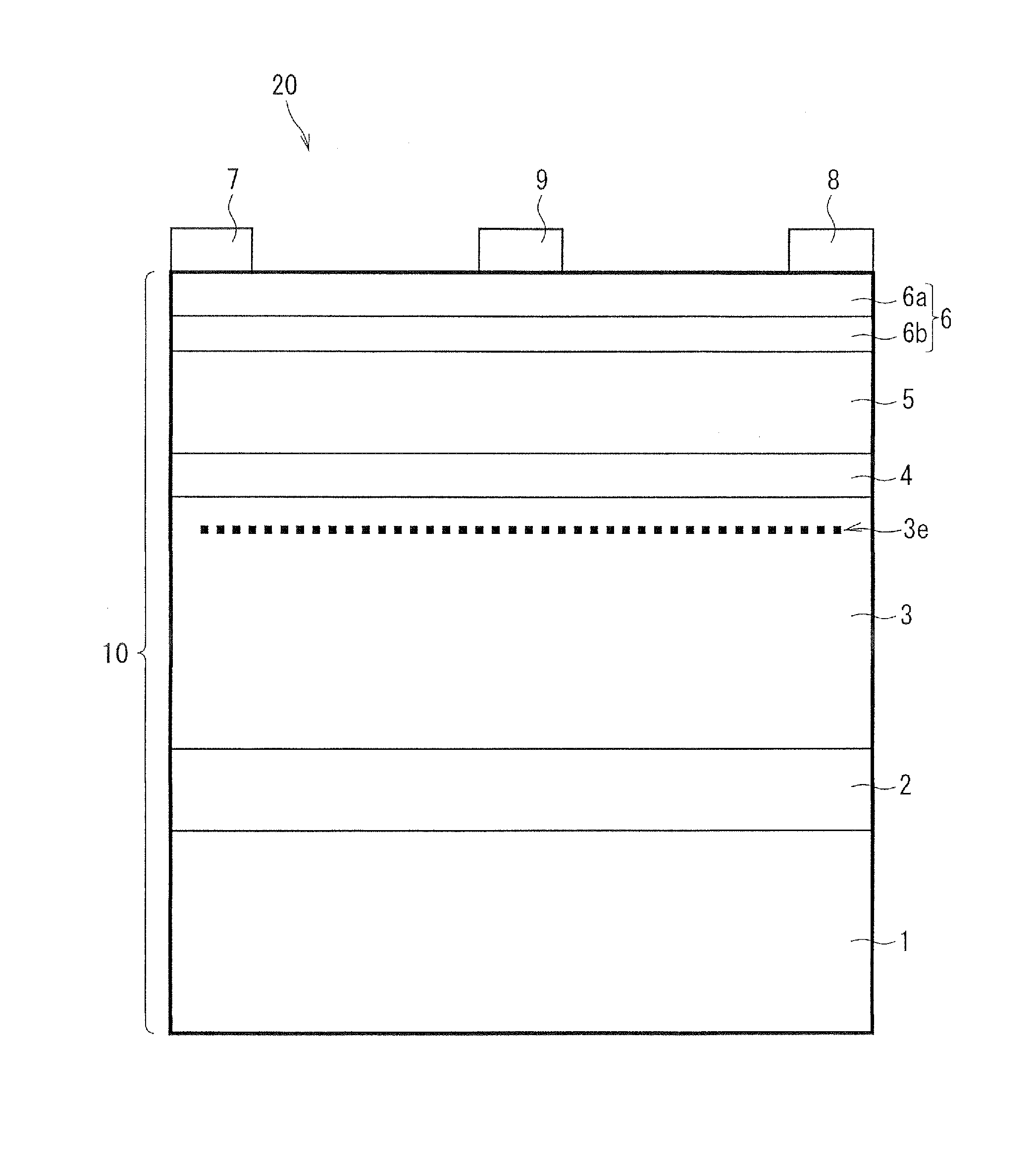
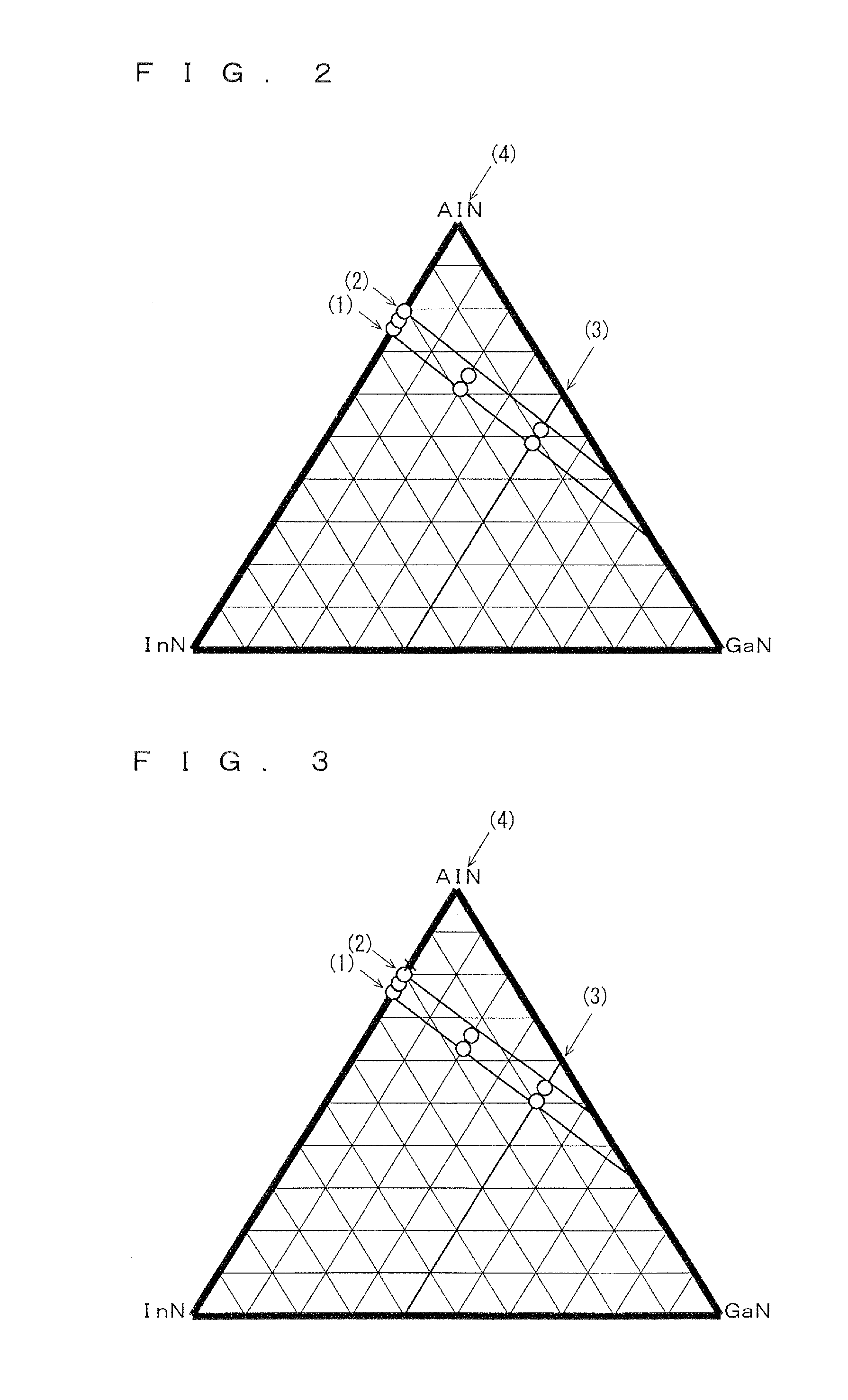

Image

  • Epitaxial substrate for semiconductor device, semiconductor device, method of manufacturing epitaxial substrate for semiconductor device, and method of manufacturing semiconductor device
  • Epitaxial substrate for semiconductor device, semiconductor device, method of manufacturing epitaxial substrate for semiconductor device, and method of manufacturing semiconductor device
  • Epitaxial substrate for semiconductor device, semiconductor device, method of manufacturing epitaxial substrate for semiconductor device, and method of manufacturing semiconductor device

Examples


example 1

[0125]In this example, as the epitaxial substrate 10 according to the above-described embodiment, 36 types of epitaxial substrates 10 were prepared which were common to one another in terms of the compositions of the channel layer 3 and the barrier layer 5 and different from one another in terms of the combination of four preparation conditions, namely, the thickness of the barrier layer 5, the thickness of the main insulating layer 6a, the formation temperature (the temperature of the susceptor) at which the main insulating layer 6a was formed, and the thickness of the sub insulating layer 6b. Then, each of the types of epitaxial substrates 10 thus obtained was measured for its sheet resistance. Moreover, each epitaxial substrate 10 was used to prepare an HEMT device 20, and its threshold voltage, contact resistance, and gate leakage current were evaluated. Table 1 shows a list of formation conditions specific to and measurement results of specimens (specimen Nos. a-1 to a-18) in w...

example 2

[0147]In this example, as the epitaxial substrate 10 according to the above-described embodiment, 28 types of epitaxial substrates 10 were prepared under the same conditions as in the example 1 except that the composition of the channel layer 3 was varied in four levels and the composition of the barrier layer 5 was varied in seven levels. Then, each of the types of epitaxial substrates 10 thus obtained was measured for its sheet resistance. Moreover, each epitaxial substrate 10 was used to prepare an HEMT device 20, and its threshold voltage, contact resistance, and gate leakage current were evaluated. In all the specimens (specimen Nos. c-1 to c-18), the thickness of the barrier layer 5 was 2 nm. The thickness of the main insulating layer 6a was 2 nm and the formation temperature (the temperature of the susceptor) at which the main insulating layer 6a was formed was 800° C. The sub insulating layer 6b was not formed. Table 3 shows a list of formation conditions specific to and mea...


PUM

PropertyMeasurementUnit
thicknessaaaaaaaaaa
thicknessaaaaaaaaaa
thicknessaaaaaaaaaa

Abstract

Provided is a semiconductor device of normally-off operation type having a low on-resistance. An epitaxial substrate for it includes: a base substrate; a channel layer made of a first group-III nitride having a composition of Inx1Aly1Gaz1N at least containing Al and Ga and x1=0 and 0≦y1≦0.3; and a barrier layer made of a second group-III nitride having a composition of Inx2Aly2Gaz2N at least containing In and Al. The composition of the second group-III nitride is, in a ternary phase diagram for InN, AlN, and GaN, in a certain range that is determined in accordance with the composition of the first group-III nitride. The barrier layer has a thickness of 3 nm or less. A low-crystallinity insulating layer is further formed on the barrier layer. The low-crystallinity insulating layer is made of silicon nitride and has a thickness of 3 nm or less.

Description

TECHNICAL FIELD[0001]The present invention relates to an epitaxial substrate having a multilayer structure made of a group-III nitride semiconductor, and particularly to an epitaxial substrate having a multilayer structure for use in a semiconductor device, to a method of manufacturing it, and to the semiconductor device.BACKGROUND ART[0002]A group-III nitride semiconductor is attracting attention as a semiconductor material for a next-generation high-frequency / high-power device, because the nitride semiconductor has a high breakdown electric field and a high saturation electron velocity. For example, an HEMT (high electron mobility transistor) device in which a barrier layer made of AlGaN and a channel layer made of GaN are laminated takes advantage of the feature that causes a high-concentration two-dimensional electron gas (2DEG) to occur in a lamination interface (hetero interface) due to the large polarization effect (a spontaneous polarization effect and a piezo polarization e...

Claims


Application Information

Patent Timeline
Patent Type & Authority Patents(United States)
IPC IPC(8): H01L21/00H01L21/02H01L29/20H01L29/66H01L29/778
CPCH01L29/778H01L29/66431H01L29/66462H01L29/7787H01L21/0262H01L21/02378H01L21/0254H01L21/0237H01L21/02458H01L29/2003H01L29/205H01L29/7786
Inventor MIYOSHI, MAKOTOICHIMURA, MIKIYATANAKA, MITSUHIRO
Owner NGK INSULATORS LTD
Learn More