Light radiating device and method of fabricating organic light emitting diode display device using the same

a light emitting diode and light beam technology, applied in the direction of identification means, instruments, manufacturing tools, etc., can solve the problems of increased production costs and sealing defects, and achieve the effect of preventing sealing defects and reducing production costs

Active Publication Date: 2014-09-30
SAMSUNG DISPLAY CO LTD
View PDF40 Cites 0 Cited by
  • Summary
  • Abstract
  • Description
  • Claims
  • Application Information

AI Technical Summary

Benefits of technology

[0009]Aspects of the present invention provide a light radiating device including a light modifier as a mask. Other aspects of the present invention provide a method of fabricating an organic light emitting diode (OLED) display device which is capable of decreasing production costs due to replacing a mask and preventing sealing defects by performing sealing using the light radiating device.

Problems solved by technology

For this reason, production costs may be increased.
Further, when the mask is not appropriately equipped, or a contaminated mask is used, sealing defects may occur.

Method used


Image

  • Light radiating device and method of fabricating organic light emitting diode display device using the same
  • Light radiating device and method of fabricating organic light emitting diode display device using the same
  • Light radiating device and method of fabricating organic light emitting diode display device using the same

Examples


Embodiment Construction

[0018]Reference will now be made in detail to exemplary embodiments of the present invention, examples of which are illustrated in the accompanying drawings, wherein like reference numerals refer to the like elements throughout. Exemplary embodiments are described below in order to explain the present invention by referring to the figures.

[0019]Hereinafter, a light radiating device and a method of fabricating an organic light emitting diode (OLED) display device according to exemplary embodiments will be described with reference to the accompanying drawings.

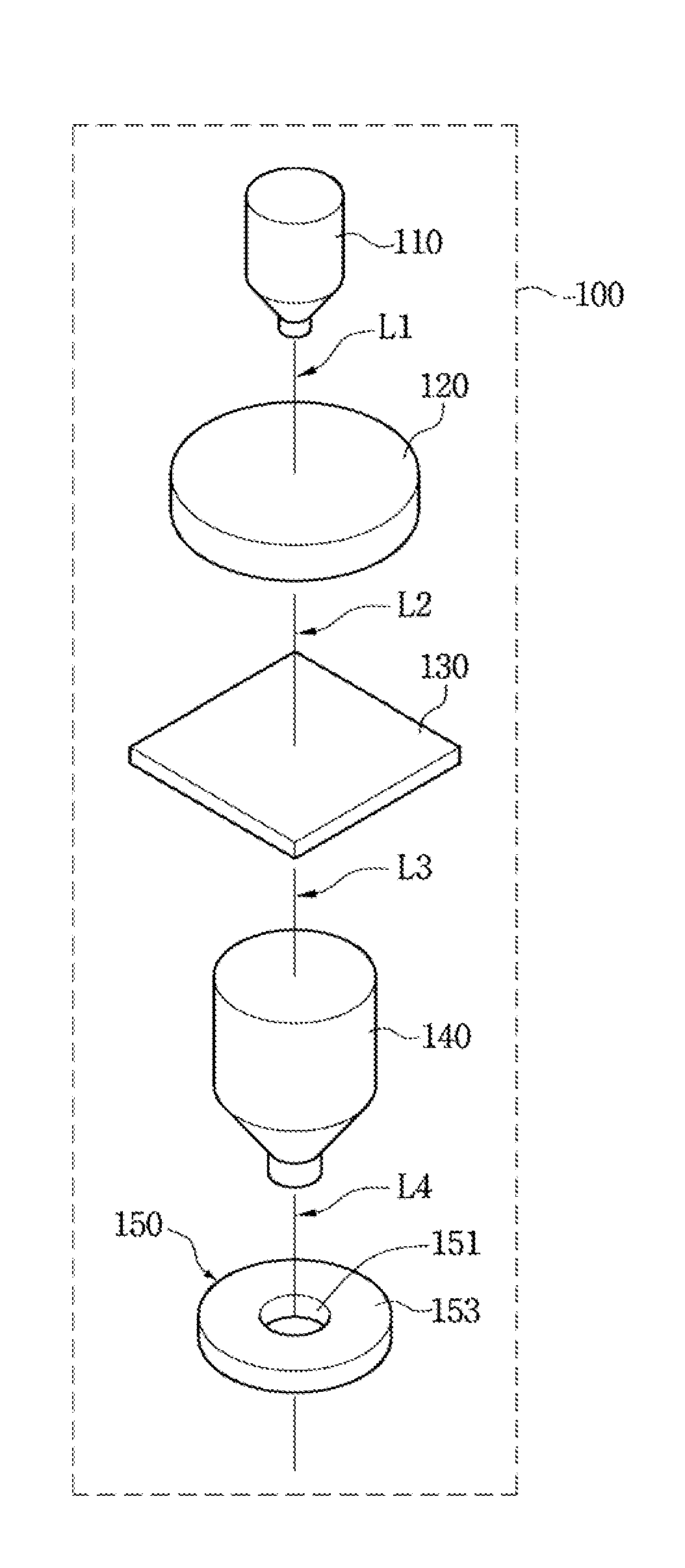
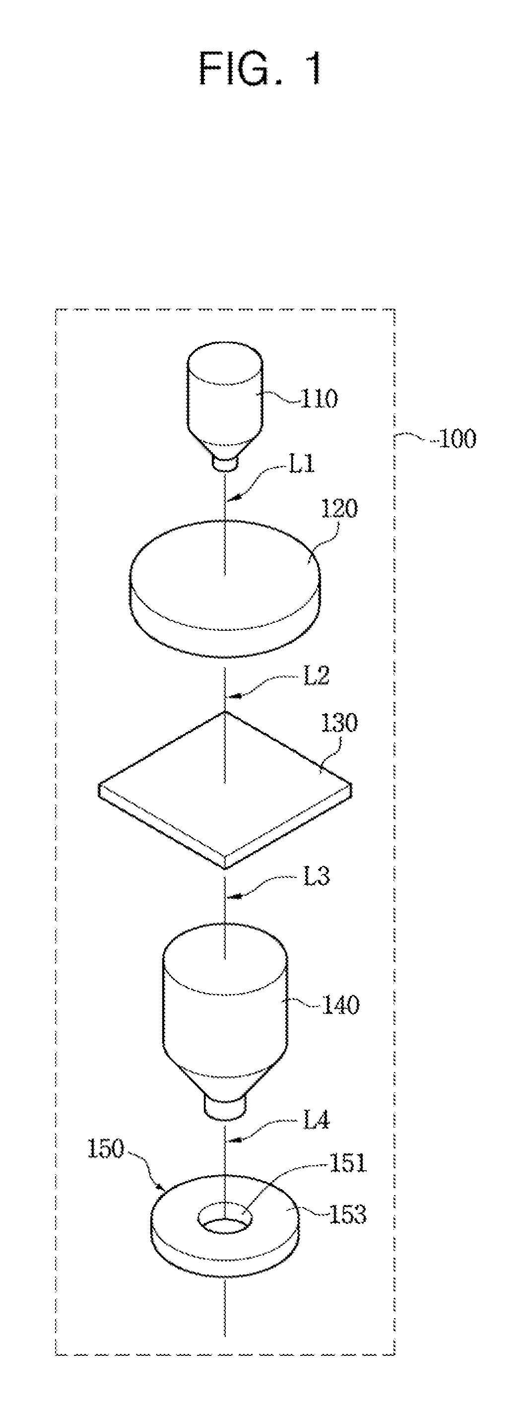
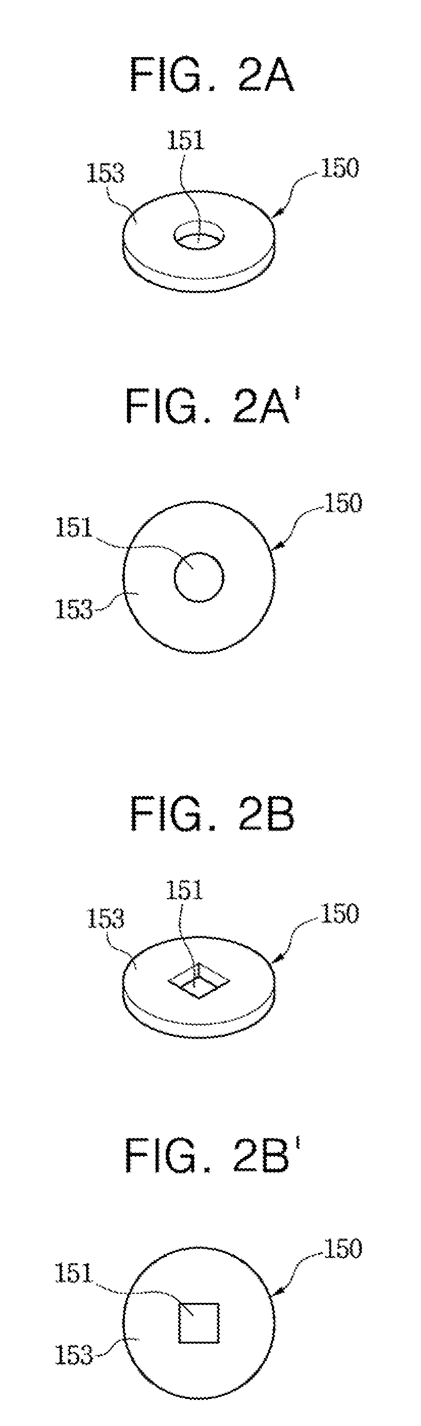
[0020]FIG. 1 is a schematic view of a light radiating device according to an exemplary embodiment, and FIGS. 2A to 3 are diagrams illustrating various figures of a light modifier included in the light radiating device according to exemplary embodiments, respectively.

[0021]Referring to FIG. 1, a light radiating device 100 includes a light source 110 to generate light, an image transformation device 120, a mask 130, a projection le...


PUM

PropertyMeasurementUnit
non-transparentaaaaaaaaaa
transparentaaaaaaaaaa
lengthaaaaaaaaaa

Abstract

A light radiating device capable of reducing production costs and preventing sealing defects for a display device, and a method of fabricating an organic light emitting diode (OLED) display device using the same are provided. The light radiating device includes a light source to generate light and a light modifier, including a transmissive region and a non-transmissive region, that define an exposure region on a substrate. The method includes applying a frit to at least one of a first substrate having a pixel region and a second substrate, plasticizing the frit, and aligning the first substrate, the second substrate, and a light radiating device to define an exposure region on the at least one of the first substrate and the second substrate, and radiating the light to the frit to couple the first substrate and the second substrate.

Description

CROSS-REFERENCE TO RELATED APPLICATION[0001]This application claims the benefit of Korean Patent Application No. 10-2009-0044169, filed May 20, 2009, in the Korean Intellectual Property Office, the disclosure of which is incorporated herein by reference.BACKGROUND OF THE INVENTION[0002]1. Field of the Invention[0003]Aspects of the present invention relates to a light radiating device capable of reducing production costs and preventing sealing defects, and a method of fabricating an organic light emitting diode display device using the light radiating device.[0004]2. Description of the Related Art[0005]Recently, among flat panel display devices, an organic light emitting diode (OLED) display device, which uses an organic light emitting diode to display moving and still pictures, has attracted attention. The OLED display device is a display device that emits light by placing an organic compound having fluorescent characteristics between electrodes, the electrodes disposed to each othe...

Claims


Application Information

Patent Timeline
Patent Type & Authority Patents(United States)
IPC IPC(8): H01S3/10B23K26/00B23K26/06G09F9/00H01L27/32H01L51/52H01L51/56H05B33/04
CPCB23K26/0656H01L51/5237B23K26/0639H01L51/56B23K26/064B23K26/066H10K71/421H10K59/8792H10K59/8722H05B33/10G02B27/62H10K50/8426H10K50/84H10K71/00
Inventor KANG, TAE-WOOK
Owner SAMSUNG DISPLAY CO LTD
Why Eureka
Try Eureka