LED encapsulation resin body, LED device, and method for manufacturing LED device
a technology of led encapsulation resin and led encapsulation resin, which is applied in the direction of basic electric elements, chemistry apparatus and processes, and light-emitting compositions. it can solve the problems of low luminous efficiency, poor heat resistance and ultraviolet resistance, and high luminous efficiency
- Summary
- Abstract
- Description
- Claims
- Application Information
AI Technical Summary
Benefits of technology
Problems solved by technology
Method used
Image
Examples
example 1
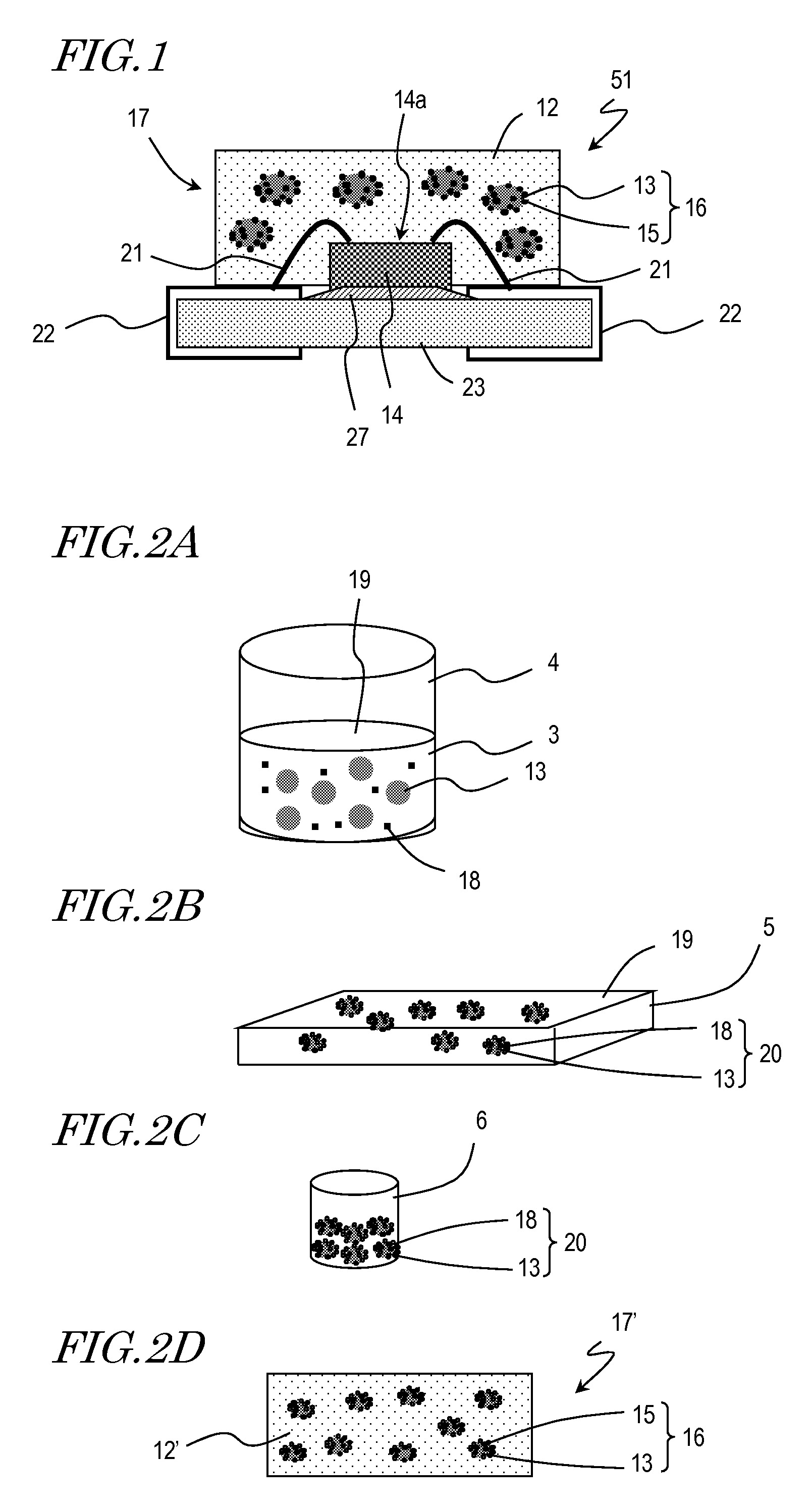
[0066]As shown in FIG. 2A, for 5 g of a strontium barium silicate-based phosphor as the phosphor 13, 1.7 g of cerium acetylacetonate (acetoacetyl) complex (cerium content: 0.15 wt %) as a metal complex 18 was put into the container (beaker) 4, and ethanol was added as the solvent 3, adjusting the entire volume to 40 ml. After the mixture 19 is stirred with a stirrer for 30 minutes, it was moved to the tray 5 and dried at 80° C. for 30 minutes, as shown in FIG. 2B. Then, as shown in FIG. 2C, the composite 20 obtained by drying was put into the crucible 6 and baked at 600° C. for 30 minutes, thereby obtaining the phosphor 13 (the composite phosphor 16) carrying cerium oxide thereon as the heat resistance material 15. The amount of cerium at this point was 0.05 wt % of the composite phosphor 16.
[0067]Next, 1.0005 g of the composite phosphor 16 was added to 5 g of the A component containing the main agent and the catalyst (hereinafter referred to as the A component) and 5 g of the B com...
example 2
[0070]The phosphor 13 carrying the heat resistance material 15 thereon (the composite phosphor 16) was obtained by a similar method to that of Example 1, using 3.4 g of a cerium acetylacetonate complex (cerium content: 0.15 wt %) with respect to 5 g of a strontium barium silicate-based phosphor. The amount of cerium at this point was 0.1 wt % of the composite phosphor 16.
[0071]Moreover, an LED encapsulation resin body (thickness: 1 mm) was produced by a similar method while adding 1.001 g of the composite phosphor 16 to 5 g of the A component and 5 g of the B component of a dimethyl silicone resin (KER-2600 manufactured by Shin-Etsu Chemical Co., Ltd.), and the ultraviolet resistance evaluation for the LED encapsulation resin body was performed. The amount of cerium at this point was 0.01 part by weight with respect to 100 parts by weight of the dimethyl silicone resin.
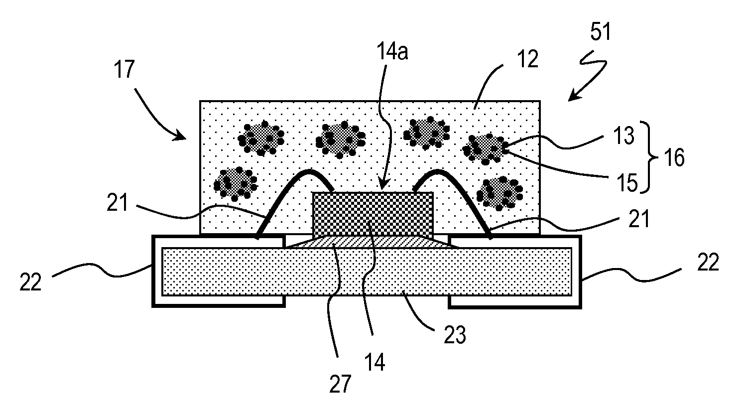
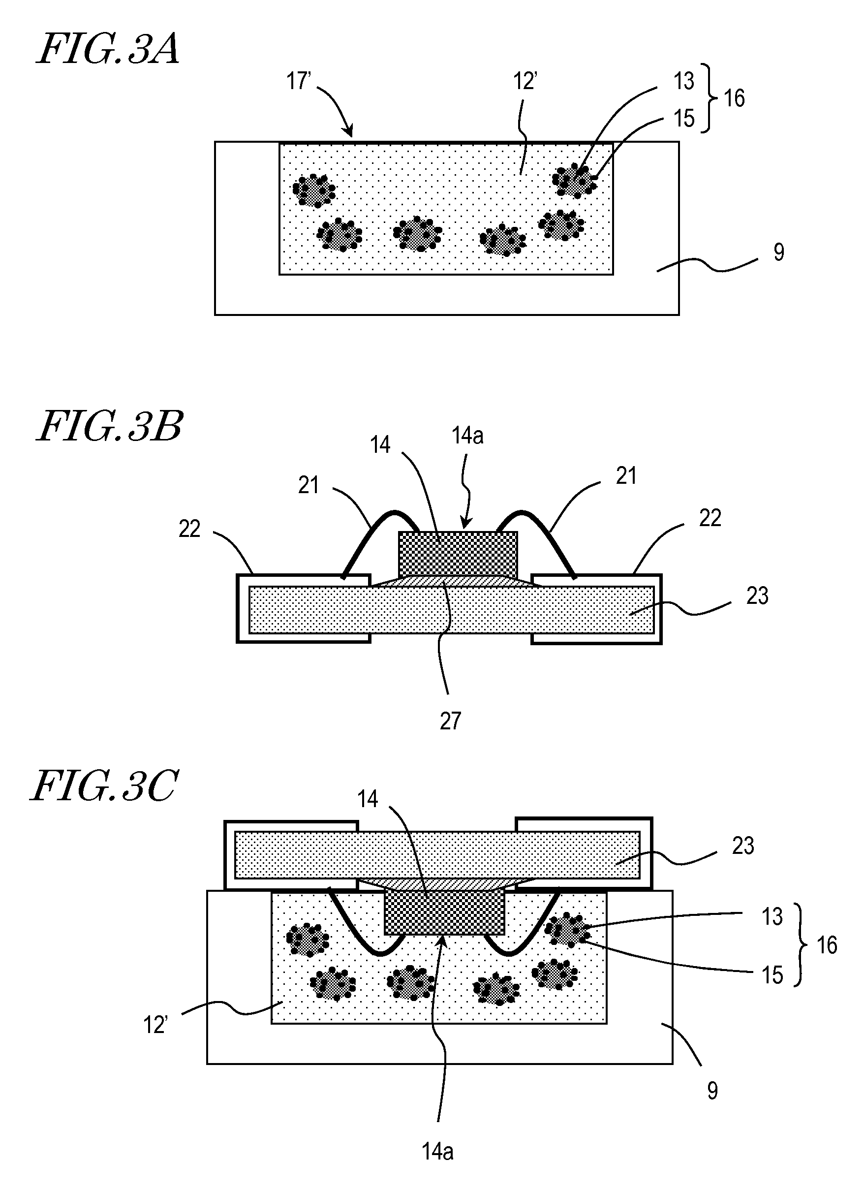
[0072]Moreover, using this LED encapsulation resin body, the LED device shown in FIG. 1 was completed by a method s...
example 3
[0073]The phosphor 13 carrying the heat resistance material 15 thereon (the composite phosphor 16) was obtained by a similar method to that of Example 1, using 17 g of a cerium acetylacetonate complex (cerium content: 0.15 wt %) with respect to 5 g of a strontium barium silicate-based phosphor. The amount of cerium at this point was 0.5 wt % of the composite phosphor 16.
[0074]Moreover, an LED encapsulation resin body (thickness: 1 mm) was produced by a similar method while adding 1.0005 g of the composite phosphor 16 to 5 g of the A component and 5 g of the B component of a dimethyl silicone resin (KER-2600 manufactured by Shin-Etsu Chemical Co., Ltd.), and the ultraviolet resistance evaluation for the LED encapsulation resin body was performed. The amount of cerium at this point was 0.05 part by weight with respect to 100 parts by weight of the dimethyl silicone resin.
[0075]Moreover, using this LED encapsulation resin body, the LED device shown in FIG. 1 was completed by a method s...
PUM
| Property | Measurement | Unit |
|---|---|---|
| size | aaaaa | aaaaa |
| temperature | aaaaa | aaaaa |
| temperature | aaaaa | aaaaa |
Abstract
Description
Claims
Application Information
 - R&D
- Intellectual Property
- Life Sciences
- Materials
- Tech Scout
- Unparalleled Data Quality
- Higher Quality Content
- 60% Fewer Hallucinations
Browse by: Latest US Patents, China's latest patents, Technical Efficacy Thesaurus, Application Domain, Technology Topic, Popular Technical Reports.
© 2025 PatSnap. All rights reserved.Legal|Privacy policy|Modern Slavery Act Transparency Statement|Sitemap|About US| Contact US: help@patsnap.com


