
ESD discharge path on chasis-mounted PCB assembly

a chasis-mounted pcb and esd technology, which is applied in the direction of printed circuit non-printed electric components, electrical apparatus casings/cabinets/drawers, instruments, etc., can solve the problem of reducing the sensitivity of esd events, ddr sdram may be corrupted, and the esd is a major reliability issue, so as to limit the scope of the claimed subject matter

Active Publication Date: 2014-06-17
AVAGO TECH INT SALES PTE LTD
View PDF3 Cites 13 Cited by
  • Summary
  • Abstract
  • Description
  • Claims
  • Application Information

AI Technical Summary

Benefits of technology

This configuration enhances the reliability of integrated circuit modules by effectively diverting ESD discharge currents away from the operational circuitry, reducing the risk of damage and ensuring uninterrupted operation.

Problems solved by technology

Electro-static discharge (ESD) is a major reliability issue in printed circuit boards and / or integrated circuits (ICs).
The large circuit current in a circuit damages the elements, conductive paths, and other parts of the IC's circuits and causes a failure during testing on some disk drives.
An example of an ESD surge problem is meeting system-level ESD testing requirements on some disk drives using a hard disk drive (HDD) controller.
Interaction between the disk drive controller and a double data rate synchronous dynamic random-access memory (DDR SDRAM) may be corrupted by the ESD surge.
If isolating the PCB assembly from the case and providing capacitive or resistive coupling to spread the discharge current flowing through the PCB assembly over time, a decrease in sensitivity to the ESD event may be provided, however, the sensitivity may not be decreased enough to meet the goals, and at high enough ESD voltages arcing from the mounting screws to nearby PCB assembly ground points may be observed.

Method used


Image

  • ESD discharge path on chasis-mounted PCB assembly
  • ESD discharge path on chasis-mounted PCB assembly
  • ESD discharge path on chasis-mounted PCB assembly

Examples


Embodiment Construction

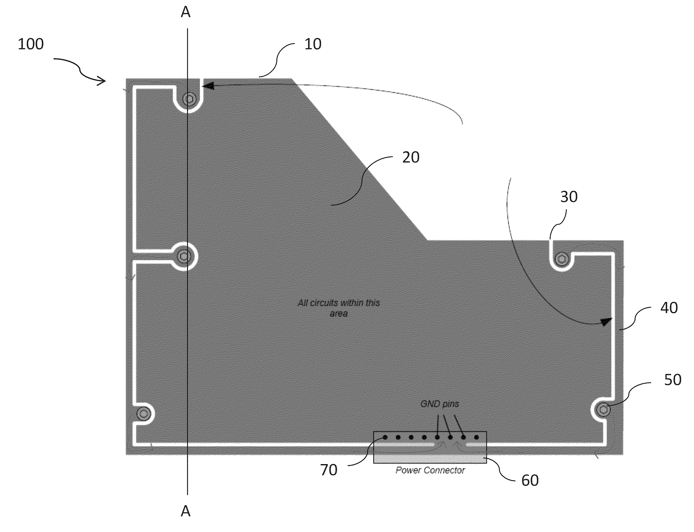
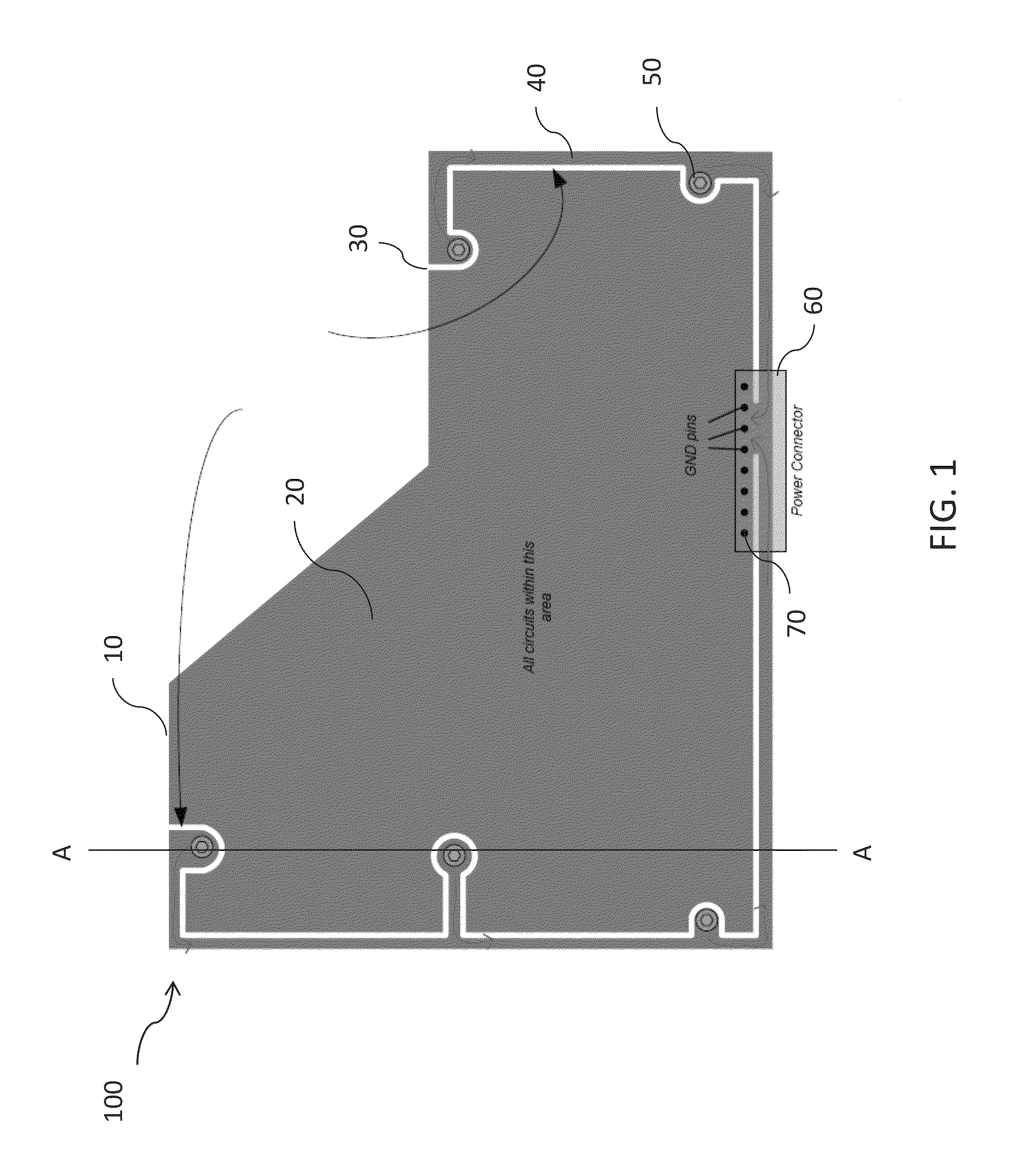
[0009]Hereinafter, embodiments of the present invention are described with reference to the drawings. In described embodiments, an ESD discharge path is provided on a chassis-mounted printed circuit board (PCB) assembly. The PCB assembly might be constructed with a separate path from chassis mounting points to a power connector ground such that charge created by, for example, and ESD discharge desirably flows through a path avoiding an area of the PCB assembly having operating circuitry. More specifically, embodiments of the present invention might provide a direct discharge path for discharging ESD current from board mounting screws to the power connector ground of the PCB assembly. Thus, a PCB assembly ground plane remains in direct contact with board mounting screws (and, thus, the case of the PCB assembly) and the power connector ground such that an ESD discharge current flows along the discharge path to reach to aground reference point, circumventing the integrated circuit modu...


PUM


Abstract

In described embodiments, a printed circuit board assembly capable of discharging electro-static discharge (ESD) surges includes an isolation trench track provided in the printed circuit board in close proximity to the peripheral edges between the peripheral edges and the mounting area, and a discharge path formed of conductive material to ground provided between the isolation trench track and the peripheral edges. The discharge path includes the board mounting screws and connects to a power connector ground of the printed circuit board.

Description

BACKGROUND OF THE INVENTION[0001]Electro-static discharge (ESD) is a major reliability issue in printed circuit boards and / or integrated circuits (ICs). ESD is a transient surge in voltage (negative or positive) that may induce a large current in. The large circuit current in a circuit damages the elements, conductive paths, and other parts of the IC's circuits and causes a failure during testing on some disk drives. To protect circuits against damage from ESD surges, various protection schemes attempt to provide a discharge path for both positive and negative ESD surges.[0002]An example of an ESD surge problem is meeting system-level ESD testing requirements on some disk drives using a hard disk drive (HDD) controller. Many experiments have been performed to understand the underlying root cause mechanism of the ESD discharge disrupting the operation of the disk drive controller. Interaction between the disk drive controller and a double data rate synchronous dynamic random-access m...

Claims


Application Information

Patent Timeline
Patent Type & Authority Patents(United States)
IPC IPC(8): H05K7/18H05K1/00H05K1/18H05K5/00H05K7/00H05K1/03
CPCH05K9/0066H05K9/0039H05K5/00G06F1/182G06F1/185
Inventor SAVORY, DAVID ALANJOHNSON, JOSHUA A.
Owner AVAGO TECH INT SALES PTE LTD
Learn More