
Method for controlling beta-tin orientation in solder joints

a technology of betatin and crystal orientation, which is applied in the direction of welding/cutting media/materials, manufacturing tools, and soldering apparatus, etc., can solve the problems of low production efficiency, low material cost, and low production efficiency, and achieve the effect of reducing material cos

Inactive Publication Date: 2014-04-22
YUAN ZE UNIV
View PDF1 Cites 0 Cited by
  • Summary
  • Abstract
  • Description
  • Claims
  • Application Information

AI Technical Summary

Benefits of technology

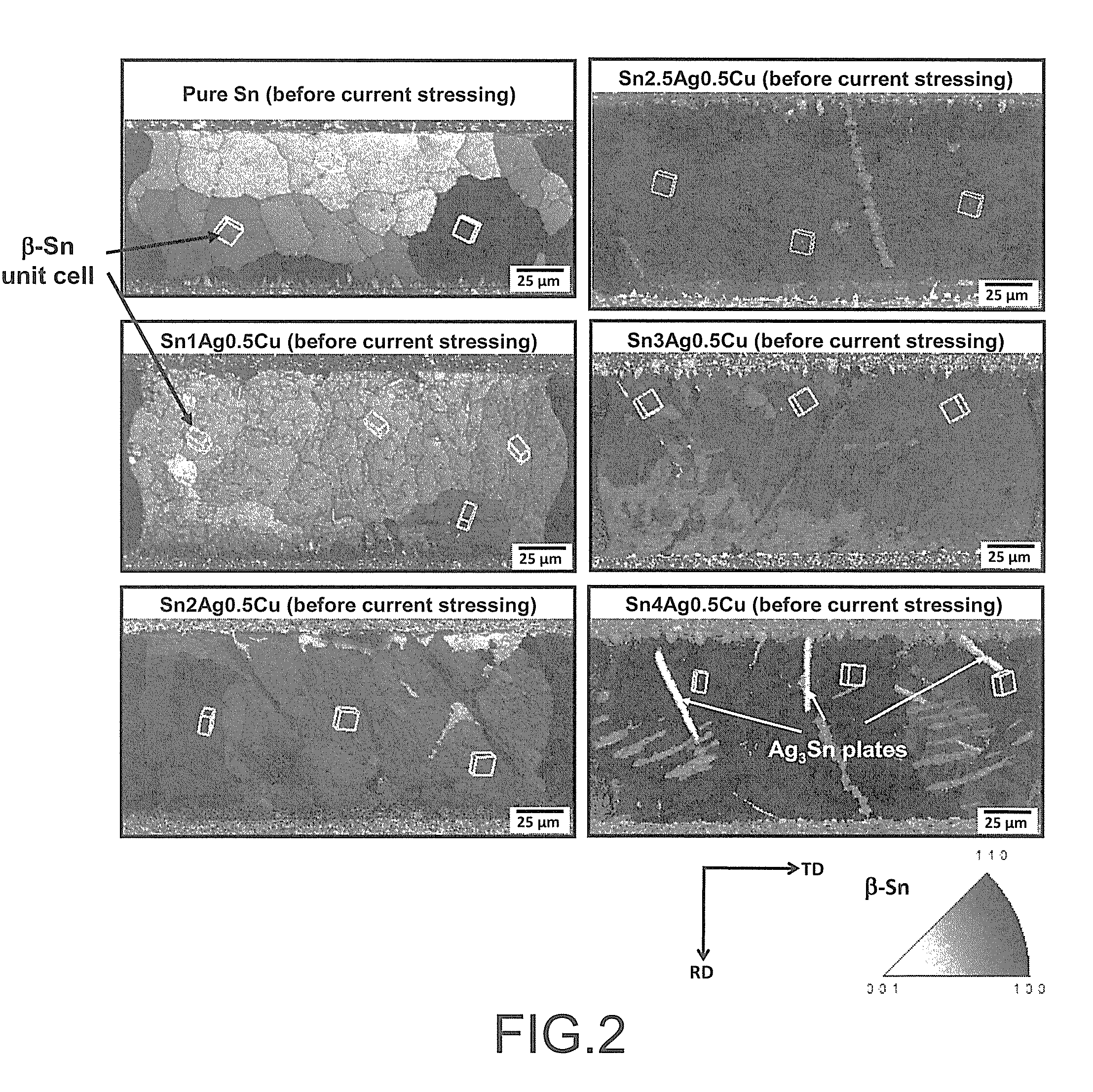
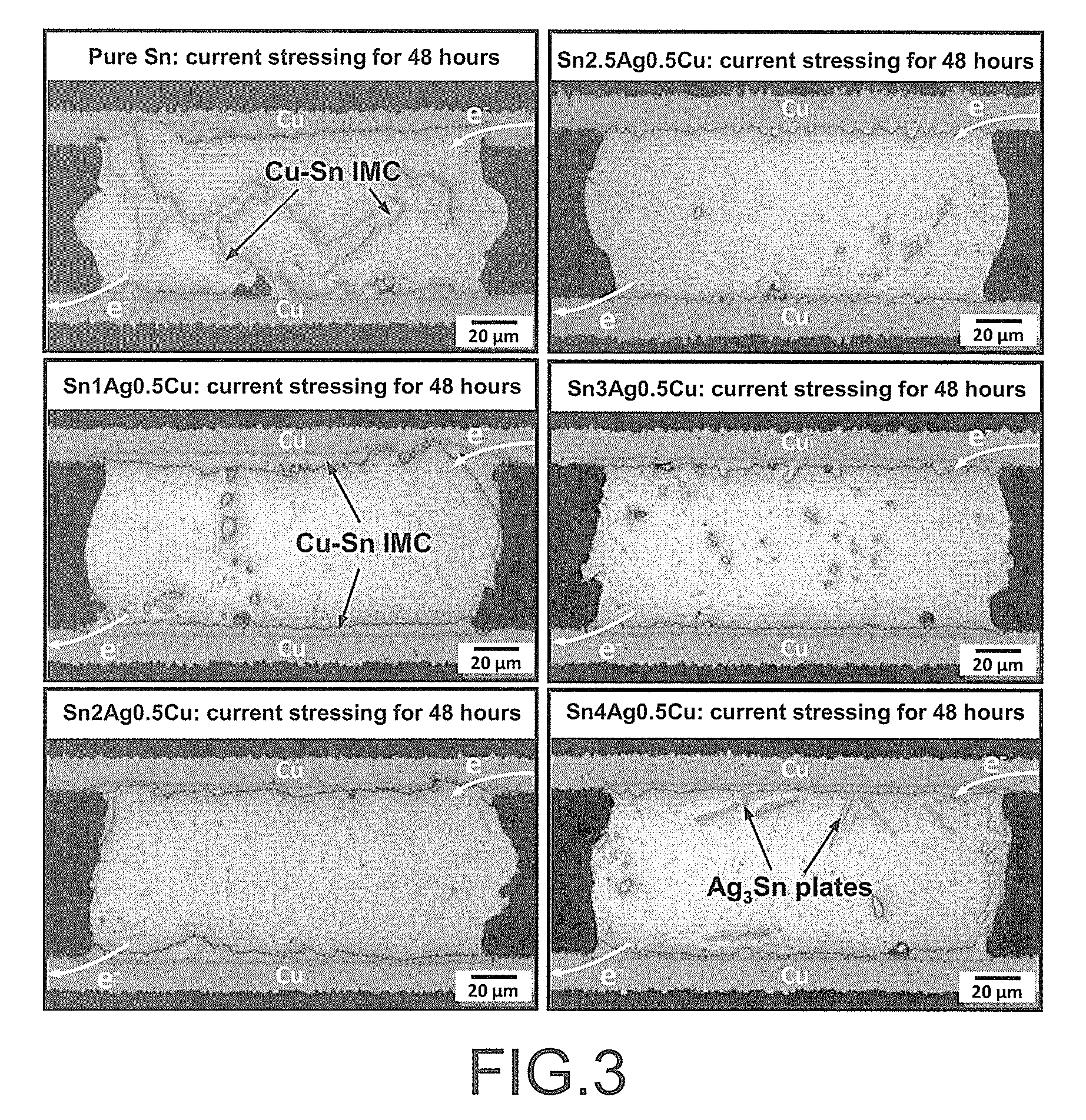
The invention is a method to control the orientation of beta-tin (β-Sn) crystals in a solder joint. The method aims to align the β-Sn crystals with the interface of the solder and metallization pad, which prevents the metallization pad from being consumed during electron current stressing. This also reduces solder deformations, the formation ofAg3Sn plates, and material cost in the soldering process. The silver content of the solder is controlled between 2.5 wt. % and 3.2 wt. %.

Problems solved by technology

These deformations in a solder enable to cause short circuit or disconnection of the solder joint, resulting in malfunction of an electronic device.
However, the thickness of the nickel surface finish is limited, so that the consumption of the film is commonly observed, especially for the solder joints experiencing a long-term electron current stressing treatment.
When the nickel film is exhausted completely, the underneath copper is then exposed to the solder and a rapid consumption in the copper metallization pads can still occur.
The exhaustion of the copper metallization pad inevitably damages the interconnections / circuits of the electronic devices and produces many fragile IMCs in the solder joints, which seriously threatens the electrical / mechanical reliability of electronic devices.
When the solder is doped with a large amount of silver, the price of such a solder material is therefore increased.
%, many Ag3Sn plates are easily created in the solder matrix, and deteriorate the mechanical properties of the solder.

Method used


Image

  • Method for controlling beta-tin orientation in solder joints
  • Method for controlling beta-tin orientation in solder joints
  • Method for controlling beta-tin orientation in solder joints

Examples


Embodiment Construction

[0023]The invention provides a solder having a specific content of silver. The solder adopts tin as the main body, where the content of silver is within the range of equal to or more than 2.5 wt. % and less than 3.2 wt. %.

[0024]Additionally, in another embodiment, the solder of the invention can further include copper or other trace elements. Here, the addition of copper to the solder enables to lower the molten temperature and to enhance the mechanical properties of the solder. The content of copper is within the range of equal to or more than 0 wt. % and less than or equal to 1.5 wt. %, for example. After the metallization pad is joined to the solder in the invention, a large consumption of the metallization pad caused by electromigration can be prevented effectively. Furthermore, joint reliability concurs such as the solder deformations can also be prevented. Detailed description is provided in the following. Generally, the material of the metallization pad is a copper-based or a...


PUM

PropertyMeasurementUnit
melting pointaaaaaaaaaa
crystal orientationaaaaaaaaaa

Abstract

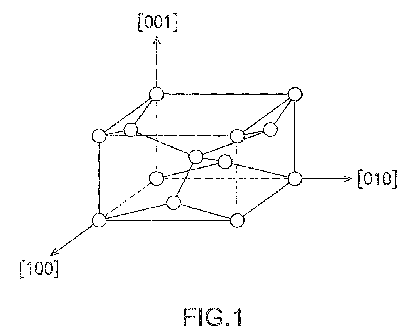
A method for controlling the beta-tin crystal orientation in solder joints is provided. The method is suitable for joining metallization pads using a solder containing tin and silver. By adjusting the silver content in the solder within a specific range of equal to or more than 2.5 wt. % and less than 3.2 wt. %, the [001] axes of beta-tin crystals in the solder is aligned to be in the direction parallel with a solder / metallization pad interface substantially. Electromigration-induced solder deformations and metallization pad consumption can be significantly reduced when solder joints have such a microstructure. Additionally, the undesired Ag3Sn plates in the solder matrix can be avoided accordingly.

Description

[0001]This application claims the priority benefit of Taiwan application serial no. 100123896, filed Jul. 6, 2011. The entirety of the above-mentioned patent application is hereby incorporated by reference herein and made a part of this specification.BACKGROUND OF THE INVENTION[0002]1. Field of the Invention[0003]The invention relates to a method for controlling the beta-tin (β-Sn) crystal orientation in solder joints, suitable for substantially enhancing the reliability of microelectronic solder joints.[0004]2. Description of Related Art[0005]Soldering is a process in which two or more metal items (hereafter termed metallization pads) are joined together using an alloy(s) with a relatively low melting temperature (hereafter termed solder), so as to achieve an electrical / mechanical connect between two (or more) components. The conventional solder utilized in the electronic industry is a binary or a multi-component alloy, which is composed of tin (Sn) and other minor elements. This i...

Claims


Application Information

Patent Timeline
Patent Type & Authority Patents(United States)
IPC IPC(8): B23K35/28
CPCB23K1/0016
Inventor HO, CHENG-ENCHEN, BO-ZONGCHEN, CHIH-NAN
Owner YUAN ZE UNIV
Learn More