
Organic light-emitting diode display and manufacturing method thereof

a technology of light-emitting diodes and organic light-emitting diodes, which is applied in the direction of discharge tube luminescnet screens, thermoelectric devices, organic semiconductor devices, etc., can solve the problems of increased “dead space” of display devices, reduce or prevent resultant damage, and efficiently control the permeation of outer moisture and oxygen , the effect of improving the life-span of organic light-emitting diodes

Active Publication Date: 2014-03-04
SAMSUNG DISPLAY CO LTD
View PDF7 Cites 6 Cited by
  • Summary
  • Abstract
  • Description
  • Claims
  • Application Information

AI Technical Summary

Benefits of technology

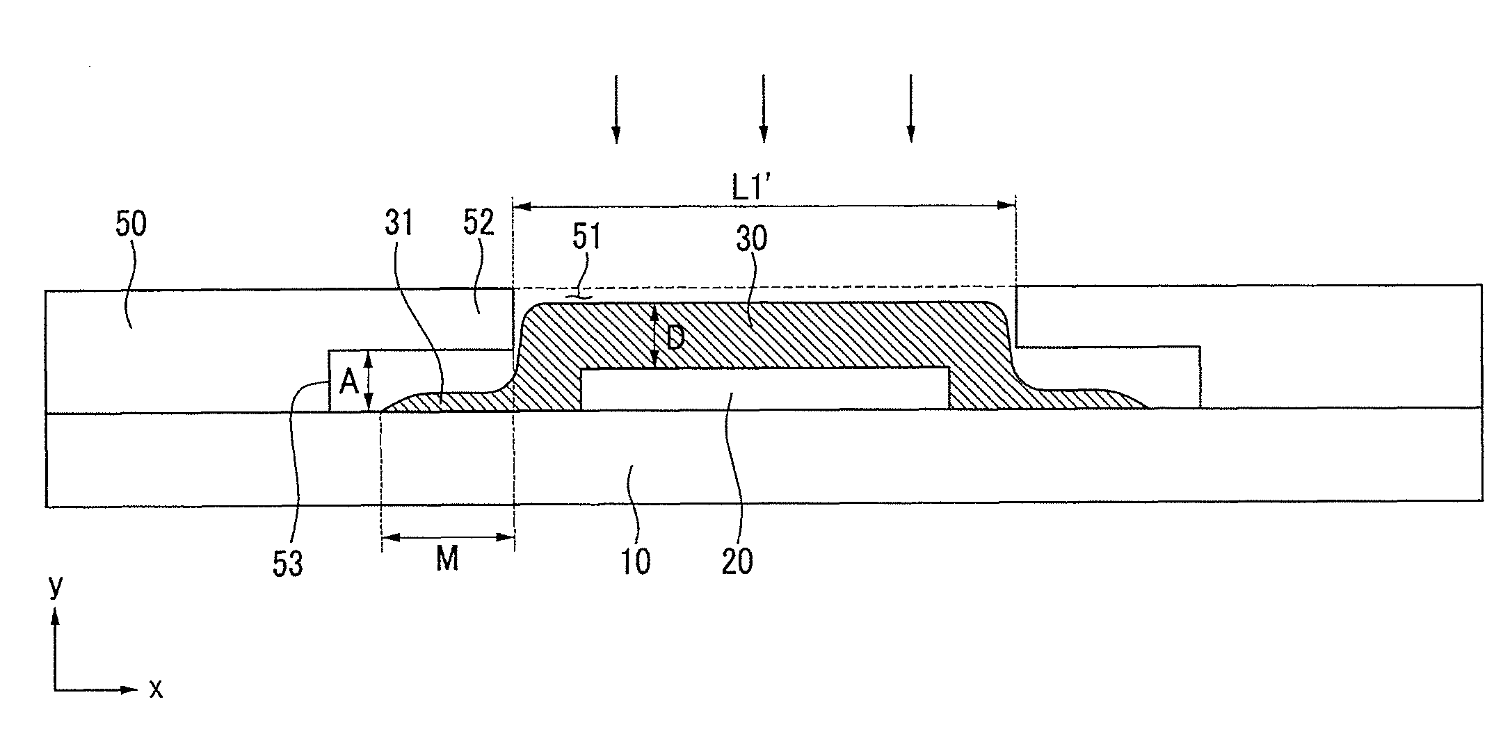
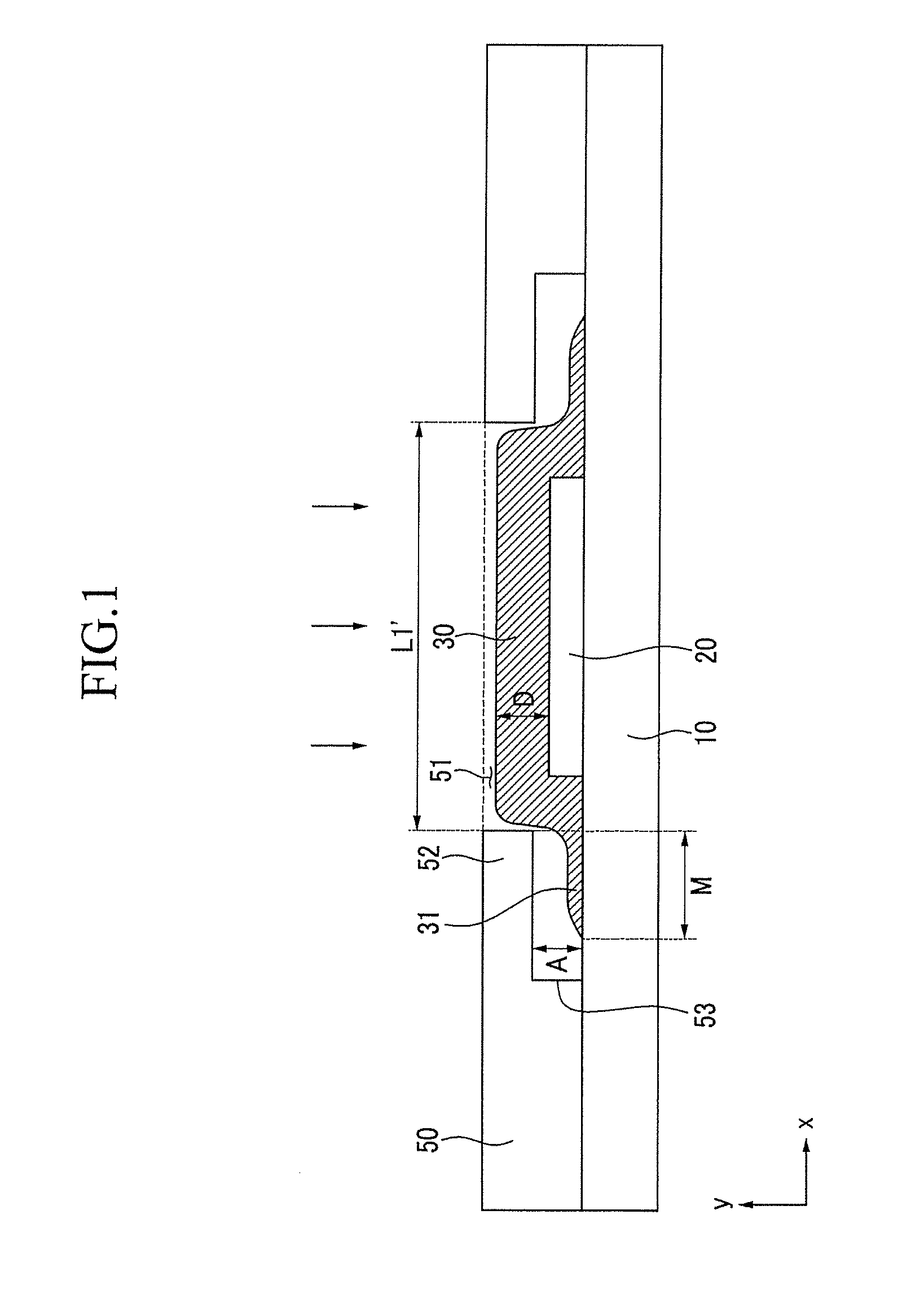
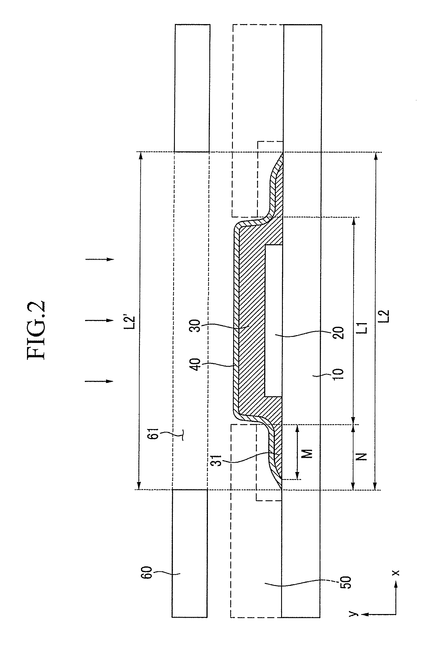
The present invention provides an OLED display that uses a special layer made of organic film and inorganic film to prevent moisture and oxygen from entering the display. This layer also reduces the space between the display and the edge, which improves its appearance. Additionally, the inorganic film is deposited in a way that minimizes its deposition area, which increases production efficiency and reduces the space between the display and its edges. The use of this special layer increases the life span of the display and reduces or eliminates dark spots. Overall, this invention prevents damage to OLED displays and improves their appearance.

Problems solved by technology

The organic light emitting diode formed with an organic material may have deteriorated performance when exposed to moisture or oxygen, and therefore, an encapsulation technique is used in the organic light emitting display panel to reduce or prevent deterioration due to moisture and oxygen.
When the deposition area of the inorganic film is extended more than needed to prevent the above-noted problem, a “dead space” of the display device is increased.

Method used


Image

  • Organic light-emitting diode display and manufacturing method thereof
  • Organic light-emitting diode display and manufacturing method thereof
  • Organic light-emitting diode display and manufacturing method thereof

Examples


experimental example

[0059]An effect of an organic light emitting diode (OLED) display according to an exemplary embodiment of the present invention will be described by comparing an organic light emitting diode (OLED) display according to a comparative example and an organic light emitting diode (OLED) display according to the exemplary embodiment of the present invention.

[0060]FIG. 6 shows a photograph of an organic light emitting diode (OLED) display that is manufactured, according to a comparative example, in a high temperature and high humidity condition, the organic light emitting diode (OLED) display being turned on, and FIG. 7 shows a photograph of an organic light emitting diode (OLED) display that is manufactured according to an exemplary embodiment of the present embodiment in a high temperature and high humidity condition, the organic light emitting diode (OLED) display being turned on.

[0061]In the comparative example of FIG. 6, the thickness (D) of the organic film is set to be 5000 Å for d...


PUM


Abstract

An organic light emitting diode display includes a substrate, an organic light emitting diode on the substrate, an organic film configured to cover the organic light emitting diode on the substrate in an organic film deposition area having a first diameter, and an inorganic film configured to cover the organic film on the substrate in an inorganic film deposition area having a second diameter, wherein L1 is the first diameter of the organic film deposition area in μm, wherein L2 is the second diameter of the inorganic film deposition area in μm, wherein D is a thickness of the organic film in μm, and wherein L2−L1≧2 (171D+150 μm).

Description

CROSS-REFERENCE TO RELATED APPLICATION[0001]This application claims priority to and the benefit of Korean Patent Application No. 10-2011-0076032 filed in the Korean Intellectual Property Office on Jul. 29, 2011, the entire content of which is incorporated herein by reference.BACKGROUND[0002]1. Field[0003]The described technology relates generally to an organic light emitting diode (OLED) display, and to a manufacturing method thereof.[0004]2. Description of Related Art[0005]An organic light emitting diode (OLED) display includes a hole injection electrode, an electron injection electrode, and an organic emission layer formed therebetween that emits light as holes injected from an anode and electrons injected from a cathode are recombined to become extinct at the organic light emission layer. The organic light emitting diode (OLED) display device, which has high quality properties such as low power consumption, high luminance, a high reaction speed, and the like, is receiving much at...

Claims


Application Information

Patent Timeline
Patent Type & Authority Patents(United States)
IPC IPC(8): H01L51/50H01L51/56
CPCH01L51/5256H01L2251/558H01L2251/55H01L51/5253H10K2102/351H10K59/8731C09K15/00H05B33/04H10K50/844H10K50/8445H10K2101/00
Inventor LEE, JAE-HO
Owner SAMSUNG DISPLAY CO LTD
Learn More