
RF power transistor circuit

a technology of power transistors and transistors, which is applied in the field of electromagnetic power devices, can solve the problems of increasing the distortion in the sideband of conventional rf power amplifiers, incurring excessive distortion and ruggedness issues, and having an upper limit to the bandwidth of input signals

Active Publication Date: 2014-02-25
NXP USA INC
View PDF8 Cites 36 Cited by
  • Summary
  • Abstract
  • Description
  • Claims
  • Application Information

AI Technical Summary

Benefits of technology

The solution significantly enhances instantaneous bandwidth and distortion correction for closely spaced signals, reducing sideband distortion and maintaining low frequency phase linearity, thus addressing the limitations of conventional RF power amplifiers.

Problems solved by technology

Conventional RF power amplifiers have an upper limit to the bandwidth of the input signal that can be amplified before incurring excessive distortion and ruggedness issues.
As signal bandwidth is increased, conventional RF power amplifiers exhibit increased distortion in the sidebands.
Additionally, high voltage excursions are present on the drain electrode of the power transistor used for amplification.
The bandwidth limitation imposed on RF power amplifiers is caused by several sources.
One source of the bandwidth limitation is due to impedance resonances loading the gate and drain of the power transistor.
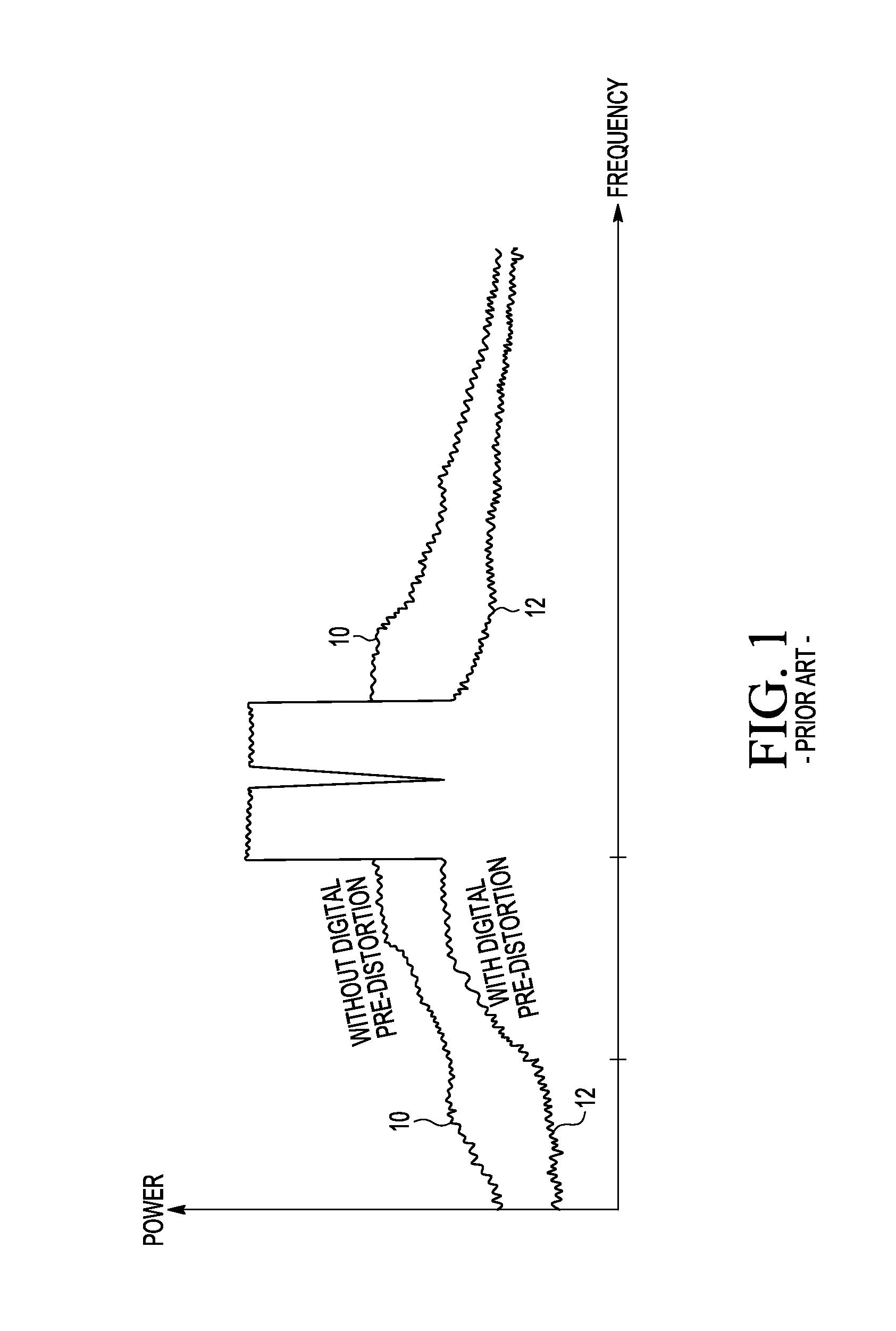
However, any kind of resonance or rapid phase transition presents a hard limit for Digital Pre-Distortion correction.
The low frequency gain peak can cause stability issues, as well as linearization problems when using a DPD system.
Conventional RF power amplifiers generally do not have all of the characteristics of very high signal bandwidth, low RF power transistor drain voltage swing, good digital pre-distortion correction and low out of band gain peaks.

Method used


Image

  • RF power transistor circuit
  • RF power transistor circuit
  • RF power transistor circuit

Examples


Embodiment Construction

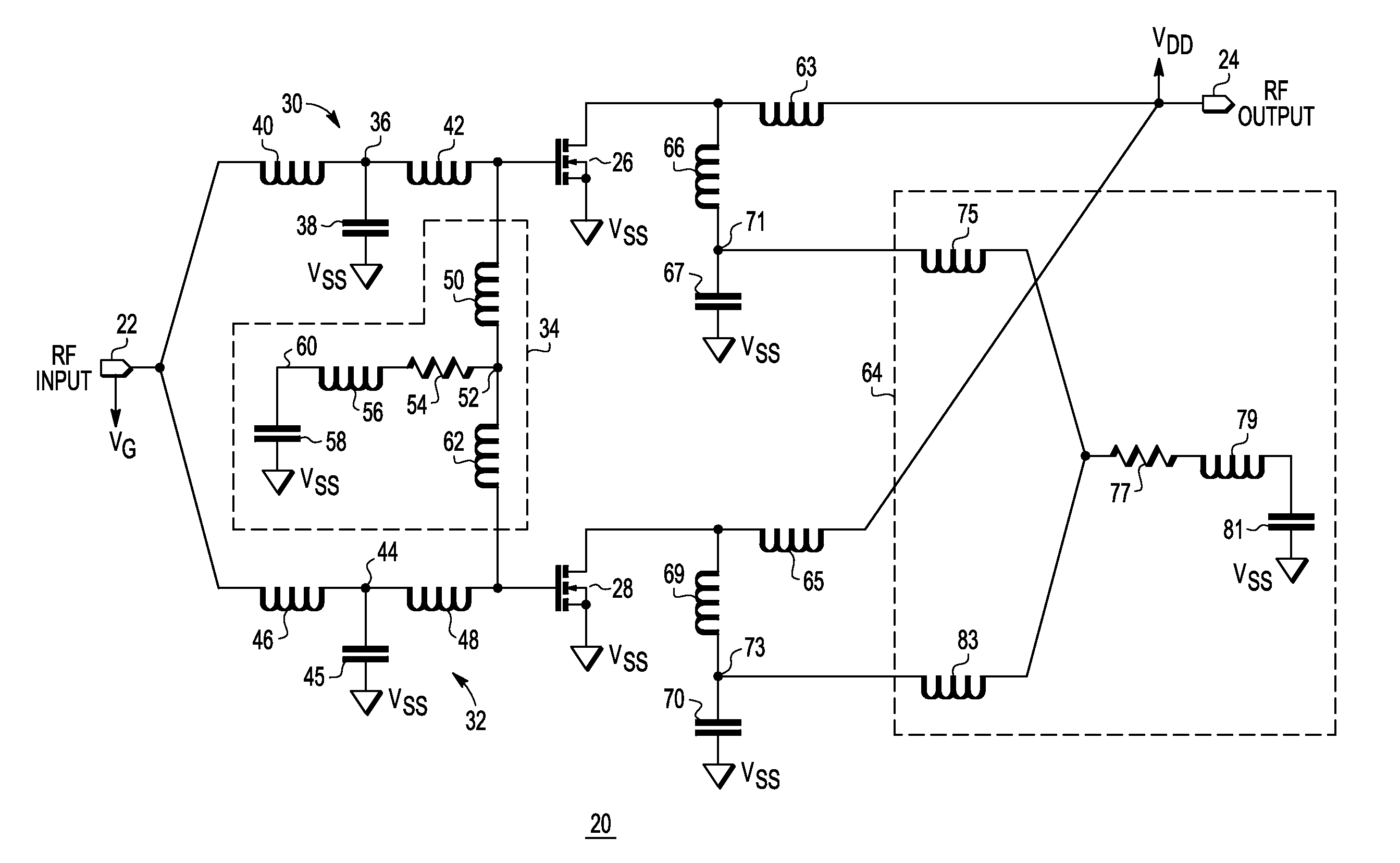
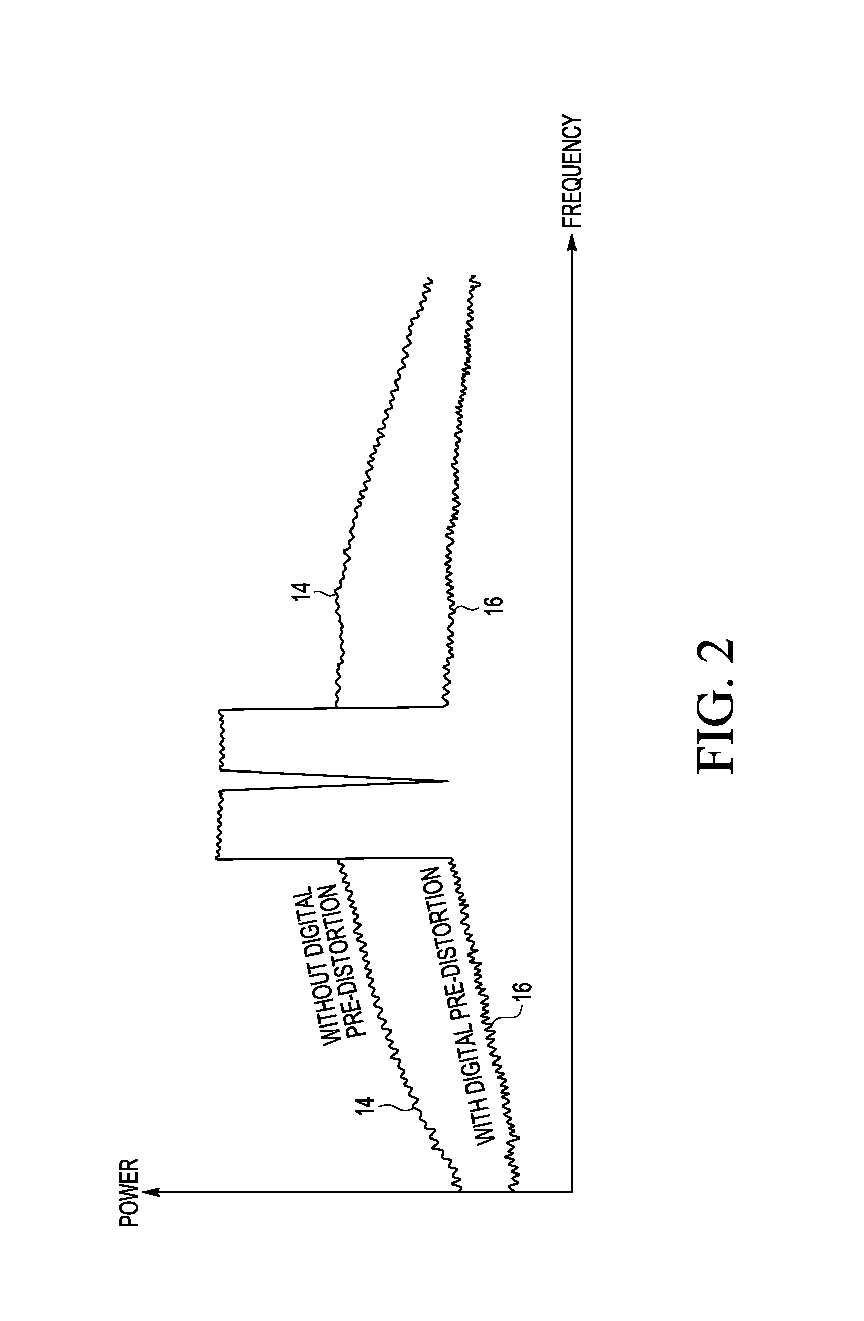
[0022]There is disclosed herein a power transistor circuit for use in a power amplifier that uses a frequency decoupling network capable of communicating high instantaneous bandwidth signals. A decoupling circuit having an inductive element, a resistive element and a capacitor is coupled together in series between a control electrode of a power transistor and a power supply terminal. The decoupling circuit dampens a resonance at a frequency lower than an RF frequency. The disclosed structure provides an RF power amplifier having low baseband impedance across an entire signal bandwidth and permits significantly increased video bandwidth. Low frequency resonance is corrected by the decoupling circuit and low frequency phase transition is eliminated to ensure good digital pre-distortion performance. The resistive element of the decoupling circuit permits pre-distortion linearization of signals with very closely spaced carriers and thus provides improved digital pre-distortion lineariza...


PUM


Abstract

A radio frequency (RF) power transistor circuit includes a power transistor and a decoupling circuit. The power transistor has a control electrode coupled to an input terminal for receiving an RF input signal, a first current electrode for providing an RF output signal at an output terminal, and a second current electrode coupled to a power supply voltage terminal. The decoupling circuit includes a first inductive element, a first resistor, and a first capacitor coupled together in series between the control electrode of the first power transistor and the power supply voltage terminal. The first decoupling circuit is for dampening a resonance at a frequency lower than an RF frequency.

Description

BACKGROUND[0001]1. Field[0002]This disclosure relates generally to semiconductors, and more specifically, to the radio frequency power devices.[0003]2. Related Art[0004]In the field of wireless communication, integrated circuits commonly implement radio frequency power amplifiers (RFPAs) which supply an amplified amount of output power. The operating frequencies for wireless communication have increased as the demand for wireless communication has increased. RF power amplifiers must have sufficient gain and bandwidth for operation well into the gigahertz range. Conventional RF power amplifiers have an upper limit to the bandwidth of the input signal that can be amplified before incurring excessive distortion and ruggedness issues. As signal bandwidth is increased, conventional RF power amplifiers exhibit increased distortion in the sidebands. Additionally, high voltage excursions are present on the drain electrode of the power transistor used for amplification. The bandwidth limitat...

Claims


Application Information

Patent Timeline
Patent Type & Authority Patents(United States)
IPC IPC(8): H03F3/04
CPCH03F1/3205H03F3/21H03F2200/391H03F1/565H03F2200/225H03F3/265H03F3/193H03F1/0288H03F1/3247H03F3/04H03F3/211H03F1/0211H03F1/42H03F2200/451H03F2203/21106
Inventor LADHANI, HUSSAIN H.BOUISSE, GERARD J.JONES, JEFFREY K.
Owner NXP USA INC
Learn More