
Epoxy resin composition for optical semiconductor device, lead frame for optical semiconductor device and substrate for optical semiconductor device obtained using the same, and optical semiconductor device

a technology of epoxy resin and semiconductor device, which is applied in the direction of semiconductor/solid-state device details, camera filters, instruments, etc., can solve the problems of optical semiconductor device becoming remarkably brittle and optical semiconductor device becoming brittle, and achieves low linear expansion coefficient and strength, and mass-produced more inexpensively.

Inactive Publication Date: 2014-01-07
NITTO DENKO CORP
View PDF7 Cites 4 Cited by
  • Summary
  • Abstract
  • Description
  • Claims
  • Application Information

AI Technical Summary

Benefits of technology

The present inventors have developed an epoxy resin composition for an optical semiconductor device that can meet both low linear expansion coefficient and strength requirements. The composition includes an epoxy resin, curing agent, white pigment, and inorganic filler. By using a silane coupling agent as a surface modifier and regulating the content of the ingredients, the composition can modify the surfaces of the white pigment and inorganic filler without causing embrittlement. This results in an optical semiconductor device that is less likely to crack or break during fabrication. The composition can be used to form a reflector for optical semiconductor devices, reducing or preventing breakage or cracking of the reflector during production.Overall, this epoxy resin composition improves the reliability and affordability of optical semiconductor devices.

Problems solved by technology

However, there is involved such a problem that if the content of the filler is increased, though the strength increases, the optical semiconductor device becomes brittle.
In particular, since the epoxy resin including an aliphatic (alicyclic) hydrocarbon as a main structure, which is used in the above-referenced Patent Document 1, is relatively poor in toughness, if a large amount of the filler is added to the material of the above-referenced Patent Document 1, there is involved such a problem that the optical semiconductor device becomes remarkably brittle.

Method used


Image

  • Epoxy resin composition for optical semiconductor device, lead frame for optical semiconductor device and substrate for optical semiconductor device obtained using the same, and optical semiconductor device
  • Epoxy resin composition for optical semiconductor device, lead frame for optical semiconductor device and substrate for optical semiconductor device obtained using the same, and optical semiconductor device
  • Epoxy resin composition for optical semiconductor device, lead frame for optical semiconductor device and substrate for optical semiconductor device obtained using the same, and optical semiconductor device

Examples


examples

[0092]Next, Examples are given below together with Comparative Examples. However, it should not be construed that the invention is limited to these Examples.

[0093]First of all, prior to the fabrication of epoxy resin compositions, materials shown below were prepared.

[Epoxy Resin (A)]

[0094]Triglycidyl isocyanurate (epoxy equivalent: 100)

[Curing Agent (B)]

[0095]4-Methylhexahydrophthalic anhydride (acid equivalent: 168)

[White Pigment (C)]

[0096]Rutile type titanium dioxide [average particle diameter: 0.21 μm, BET specific surface area (X1): 9.0 m2 / g]

[Inorganic Filler (D)]

[0097]Spherical fused silica [average particle diameter: 22 μm, BET specific surface area (Y1): 3.2 m2 / g]

[Silane Coupling Agent (E)]

[0098]3-Glycidoxypropyl trimethoxysilane [minimum coverage area (Z1): 330 m2 / g]

[Curing Accelerator (F)]

[0099]Tetra-n-butylphosphonium-o,o-diethylphosphorodithioate


PUM

PropertyMeasurementUnit
wavelength rangeaaaaaaaaaa
light reflectivityaaaaaaaaaa
flexural elastic modulusaaaaaaaaaa

Abstract

The present invention relates to an epoxy resin composition for an optical semiconductor device, including the following ingredients (A) to (E): (A) an epoxy resin; (B) a curing agent; (C) a white pigment; (D) an inorganic filler; and (E) a silane coupling agent, in which a total content of the ingredient (C) and the ingredient (D) is from 69 to 94% by weight of the whole of the epoxy resin composition, and the ingredient (E) is contained in an amount satisfying the specific conditions.

Description

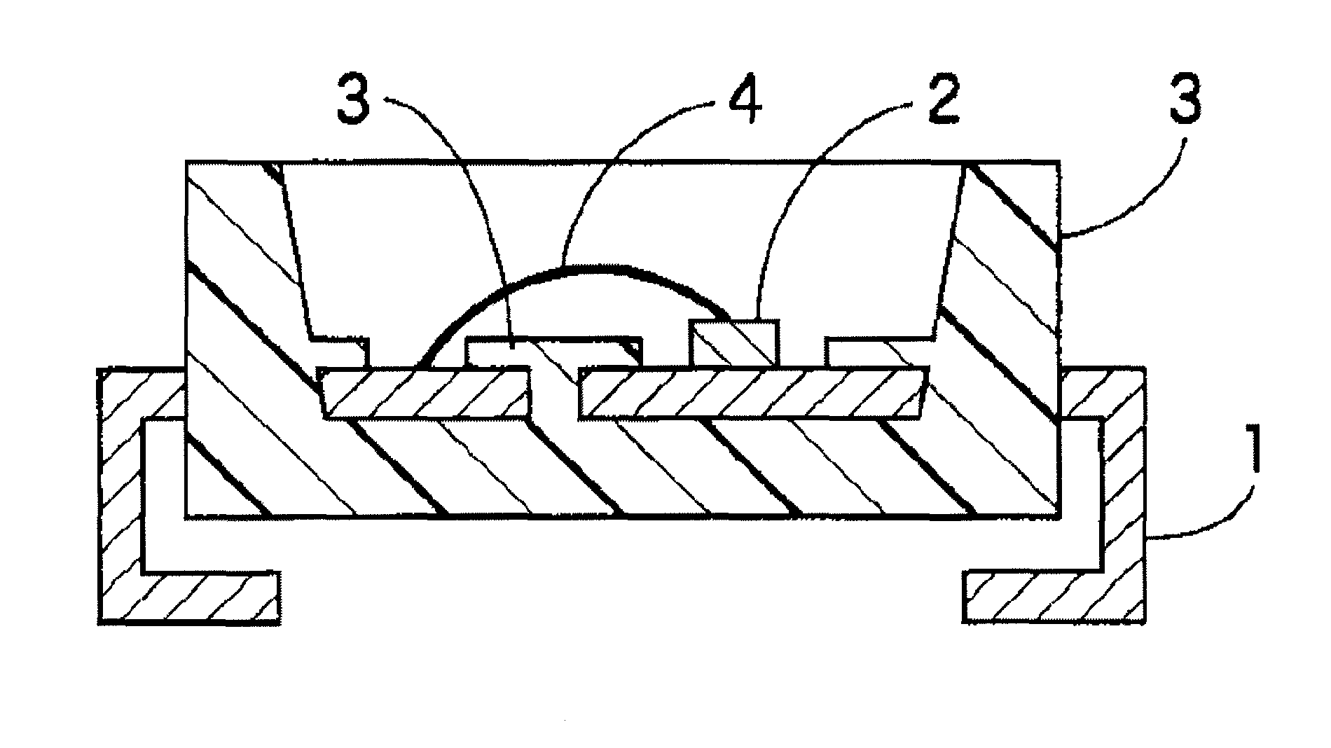
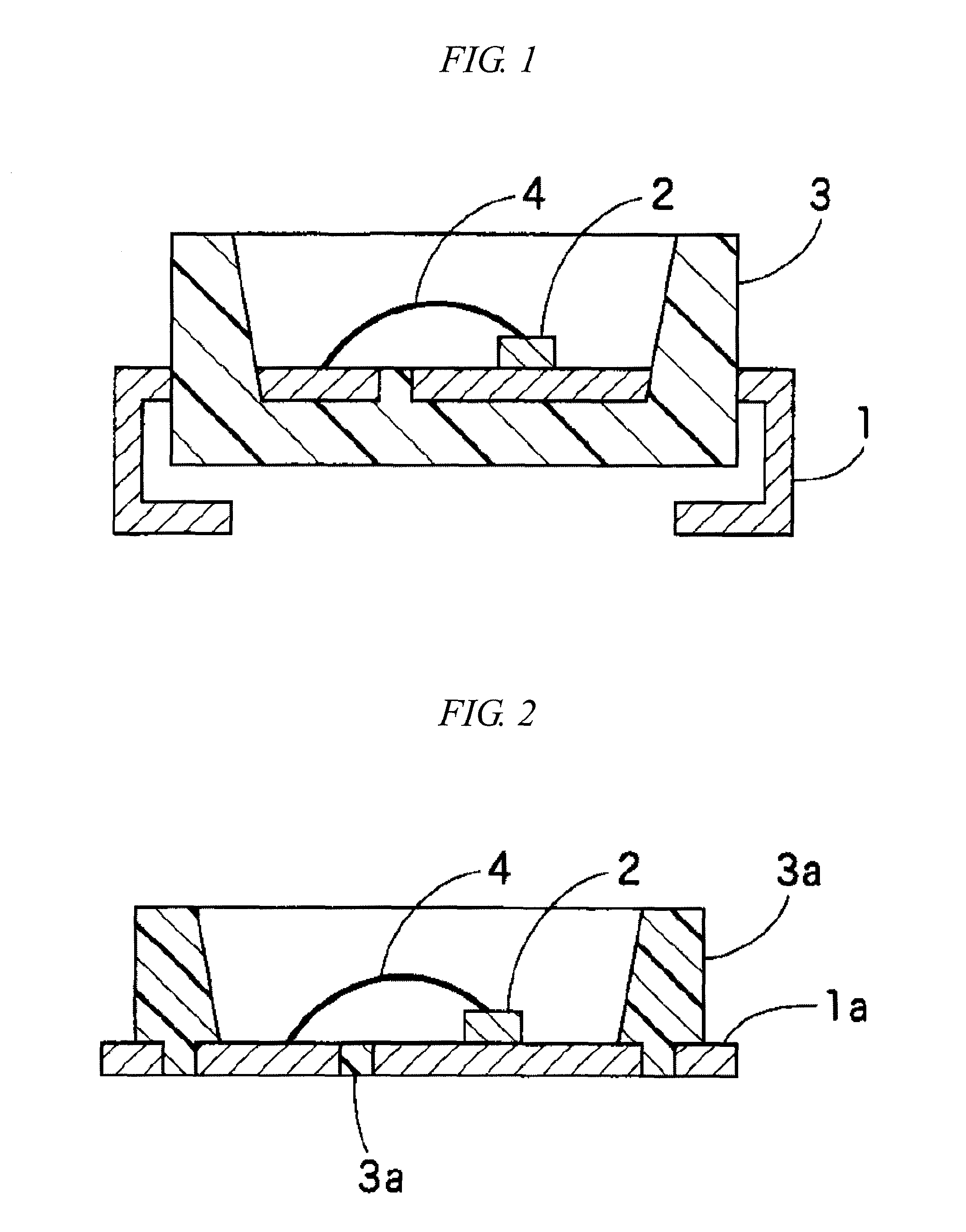
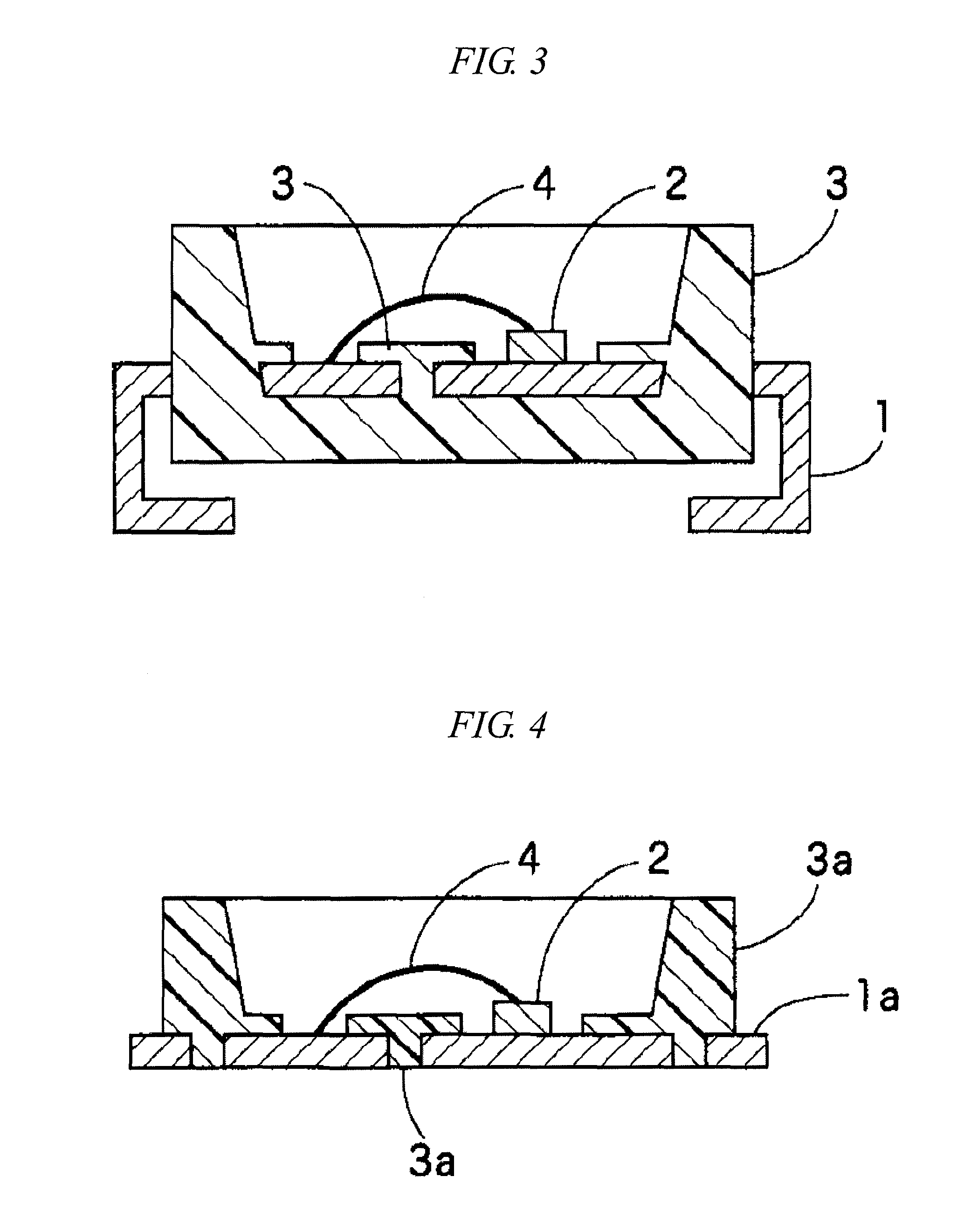
FIELD OF THE INVENTION[0001]The present invention relates to an epoxy resin composition for an optical semiconductor device which is used as a material for forming a reflector (reflection part) that reflects light emitted from, for example, an optical semiconductor element. The invention further relates to a lead frame for an optical semiconductor device and a substrate for an optical semiconductor device, obtained using the epoxy resin composition and relates to an optical semiconductor device.BACKGROUND OF THE INVENTION[0002]Conventional optical semiconductor devices including an optical semiconductor element mounted therein have a configuration including a metallic lead frame 1, an optical semiconductor element 2 mounted thereon, and a reflector 3 for light reflection formed of a resin material so as to surround the periphery of the optical semiconductor element 2, as shown in FIG. 1. Then, a space including the optical semiconductor element 2 surrounded by the reflector 3 is enc...

Claims


Application Information

Patent Timeline
Patent Type & Authority Patents(United States)
IPC IPC(8): H01L31/0203
CPCC08K3/36H01L33/486H01L2924/3025C08K3/22C08K5/548H01L2224/48247H01L33/60C08L63/00H01L2224/48091C08K5/5435C08K5/544C08K2003/2241C08K5/54H01L2924/00014H01L2924/00H01L33/10
Inventor FUKE, KAZUHIROONISHI, HIDENORIOTA, SHINYA
Owner NITTO DENKO CORP
Learn More