Semiconductor optical modulator, semiconductor optical integrated device, and method of manufacturing the same

a semiconductor optical and integrated device technology, applied in the direction of instruments, non-linear optics, optical elements, etc., can solve the problems of low optical loss, inability to increase the extinction ratio as the mz optical modulator, and difficulty in simultaneously realizing the great change in refractive index, etc., to achieve the effect of low optical loss

Inactive Publication Date: 2013-12-03
NEC CORP
View PDF9 Cites 7 Cited by
  • Summary
  • Abstract
  • Description
  • Claims
  • Application Information

AI Technical Summary

Benefits of technology

[0016]However, when the rib waveguide is applied to the semiconductor MZ optical waveguide, it is found that there is an issue that it is difficult to simultaneously realize the great change in the refractive index, the low optical loss, and the suppression of a high-order mode upon applying an electric field.
[0017]In order to satisfy the condition of the great change in the refractive index and the low loss, the number of a well layer increases so as to realize a sufficient change in a refractive index even in a low electric field. In order to reduce an operation voltage, a thickness and number of a well layer in the core layer are set such that the thickness is increased, and the number is increased in general. Specifically, the core layer structure having a strong optical confinement is advantageous for improving the characteristic. It has also been known that an optical absorption gradually increases in general over a predetermined electric field. From this, a strong optical confinement structure is effective for reducing insertion loss.
[0022]The present invention is accomplished in view of the above-mentioned circumstance, and an exemplary object of the invention is to provide a semiconductor optical modulator that is excellent in an electric-field applying efficiency and a single mode characteristic.
[0039]The present invention can provide a semiconductor optical modulator that is excellent in an electric-field applying efficiency and a single mode characteristic.

Problems solved by technology

However, when the rib waveguide is applied to the semiconductor MZ optical waveguide, it is found that there is an issue that it is difficult to simultaneously realize the great change in the refractive index, the low optical loss, and the suppression of a high-order mode upon applying an electric field.
On the other hand, from the viewpoint of forming a single mode waveguide, the structure having a strong optical confinement is undesirable.
However, if there is a high-order mode, a phase rotation amount to the applied electric field is different for every mode, so that an extinction ratio cannot be increased as the MZ optical modulator.
On the contrary, when the waveguide structure satisfying the condition of setting a single mode is used, the operation voltage increases, and the insertion loss increases, which means the performance as the MZ modulator is deteriorated.
Accordingly, the semiconductor MZ optical modulator having a satisfactory characteristic cannot be realized by using the rib waveguide, if this goes on.

Method used


Image

  • Semiconductor optical modulator, semiconductor optical integrated device, and method of manufacturing the same
  • Semiconductor optical modulator, semiconductor optical integrated device, and method of manufacturing the same
  • Semiconductor optical modulator, semiconductor optical integrated device, and method of manufacturing the same

Examples


example 1

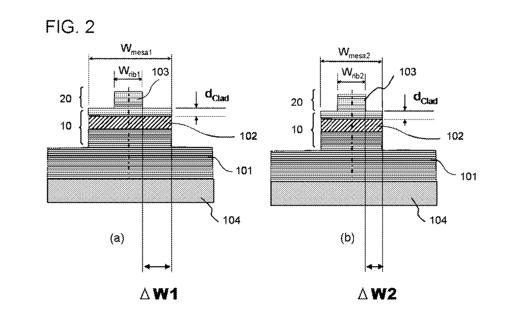
[0106]A two-step mesa optical waveguide constituting the semiconductor optical modulator according to the present invention was manufactured. The sectional view of the two-step mesa optical waveguide is the same as that in FIG. 2. The manufacturing procedure is the same as that illustrated in FIGS. 3 and 4.

[0107]An InGaAlAs / InGaAlAs core layer 102 having 10 well layers with a width of the well of 10 nm was epitaxially grown on an n-InP substrate 109. The InGaAlAs / InGaAlAs core layer 102 has a high optical confinement exceeding 60 nm, which is the reference, wherein the a in the equation (9) is 66, the product of the number of the wells and the width of the well is 100 nm. The first clad layer 101 employed n-InP, while the second clad layer 103 employed p-InP.

[0108]FIG. 3(a) illustrates a sectional view in which the mask 105 was formed. The thickness of the second clad layer 103 was 2 μm including the InGaAs serving as the contact layer. Then, an etching was carried out with a dry et...

example 2

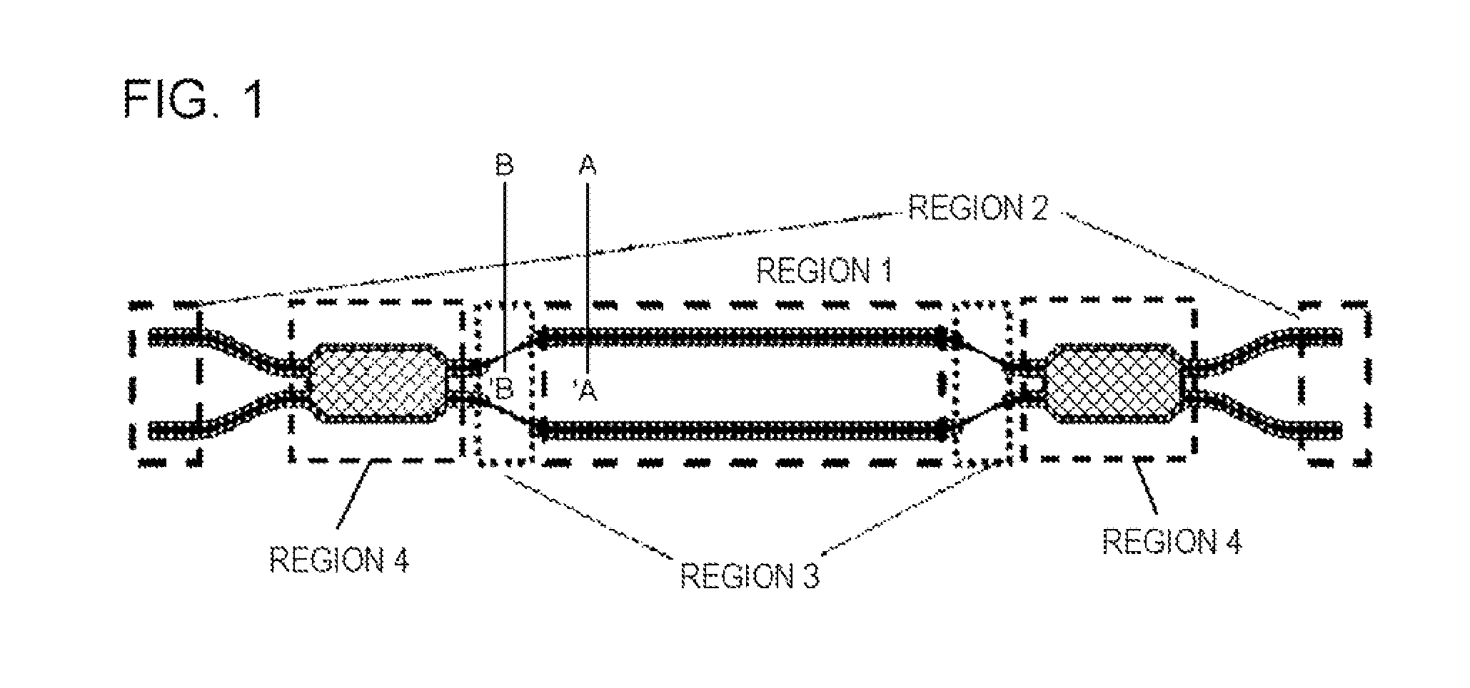
[0113]A semiconductor MZ interference optical modulator, which was one example of the semiconductor optical modulator according to the present invention, was manufactured. The top view of the semiconductor MZ interference optical modulator according to the present exemplary embodiment is the same as that in FIG. 1. The optical modulator in the present exemplary embodiment is also composed of a two-step mesa optical waveguide. The sectional view of the two-step mesa optical waveguide is the same as that in FIG. 2. The manufacturing procedure is the same as that illustrated in FIGS. 3 and 4.

[0114]An InGaAlAs / InGaAlAs core layer 102 having 10 well layers with a width of the well of 10 nm was epitaxially grown on an n-InP substrate 104. The InGaAlAs / InGaAlAs core layer 102 has a high optical confinement exceeding 60 nm, which is the reference, wherein the a in the equation (4) is 66, the product of the number of the wells and the width of the well is 100 nm. The first clad layer 101 emp...


PUM

PropertyMeasurementUnit
widthaaaaaaaaaa
mesa widthaaaaaaaaaa

Abstract

The invention provides a semiconductor optical modulator including a two-step mesa optical waveguide having a first clad layer (101); a mesa-like core layer (102) formed over the first clad layer (101); and a second clad layer (103) formed into a mesa shape over the core layer (102), and having a mesa width smaller than that of the core layer (102). The two-step mesa optical waveguide includes a multi-mode optical waveguide region to which an electric field is applied or into which an electric current is injected, and a single-mode optical waveguide region to which the electric field is not applied and into which the electric current is not injected. When the mesa width of the core layer in the multi-mode optical waveguide region is defined as Wmesa1, and the mesa width of the core layer in the single-mode optical waveguide region is defined as Wmesa2, Wmesa1>Wmesa2 is satisfied.

Description

TECHNICAL FIELD[0001]The present invention relates to a semiconductor optical modulator, a semiconductor optical integrated device using the same, and a method of manufacturing the same.BACKGROUND ART[0002]In a wavelength division multiplexing (WDM) in a trunk-line, a modulation speed and a transmission capacity have been increased. An optical modulator used in this system has been desired not only that it is driven with a low voltage and it is operated with high modulation speed, but also that it is compact, an optical modulating characteristic does not depend upon a wavelength, and it is compatible with a multilevel coding modulation, which has a high use efficiency of a band.[0003]The optical modulating system that is currently put into practical use is classified, from a viewpoint of modulation principle, into a system directly modulating a light source (laser), an electro absorption optical modulator, and an optical modulator (Mach-Zehnder optical modulator) utilizing a Mach-Ze...

Claims


Application Information

Patent Timeline
Patent Type & Authority Patents(United States)
IPC IPC(8): G02F1/035G02F1/01G02B6/10H01L21/00H01L33/00
CPCG02F1/2257G02F2201/063G02F2201/05G02F2001/212G02F1/212
Inventor SUDO, SHINYAKATO, TOMOAKISATO, KENJIMORIMOTO, TAKAO
Owner NEC CORP
Why Eureka
Try Eureka