Pentacene-carbon nanotube composite, method of forming the composite, and semiconductor device including the composite

a carbon nanotube and composite material technology, applied in the field of composite materials, can solve the problems of carbon nanotubes, difficult to fabricate integrated circuits, and limited charge carrier mobility of organic thin film transistors (ofets)

Active Publication Date: 2013-12-03
GLOBALFOUNDRIES U S INC
View PDF13 Cites 12 Cited by
  • Summary
  • Abstract
  • Description
  • Claims
  • Application Information

AI Technical Summary

Benefits of technology

The present invention is about a method of making a semiconductor device by using a carbon nanotube-pentacene composite layer as the channel region. This method involves depositing a dispersion of pentacene precursor and carbon nanotubes on a substrate, heating it to remove the solvent and convert the precursor to pentacene, thereby forming the composite layer. This method can be used in making field effect transistors by creating source, drain, and gate electrodes on a substrate with the channel region containing the carbon nanotube-pentacene composite layer. The unique features of this invention make it possible to create semiconductor devices with improved performance.

Problems solved by technology

However, the charge carrier mobility of these organic thin film transistors (OFET) are limited and usually in the range of 10−2 cm2 / V·sec to 10−1 cm2 / V·sec.
On the other hand, carbon nanotubes have been demonstrated to have charge carrier mobility far superior to that of single crystal silicon but are very difficult to fabricate integrated circuits.

Method used


Image

  • Pentacene-carbon nanotube composite, method of forming the composite, and semiconductor device including the composite
  • Pentacene-carbon nanotube composite, method of forming the composite, and semiconductor device including the composite
  • Pentacene-carbon nanotube composite, method of forming the composite, and semiconductor device including the composite

Examples


examples

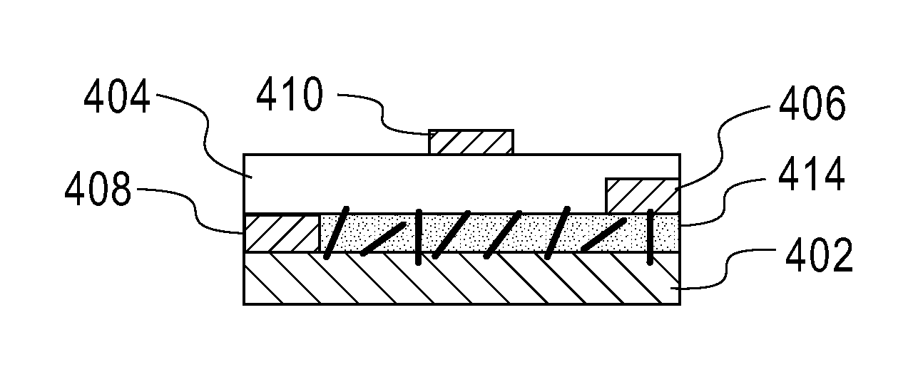
[0046]FIG. 4 illustrates an exemplary method 400 of forming a semiconductor device 450 (e.g., field effect transistor (FET)) according an exemplary aspect of the present invention.

[0047]As illustrated in FIG. 4, a substrate 402 (e.g., semiconductor substrate such as silicon, germanium, etc.) may be provided with a gate electrode 410 (e.g., highly doped silicon), an insulation layer 404 (e.g., SiO2, SiN, SiON), and a source electrode 406 (e.g., gold, palladium, etc.) and a drain electrode 408 (e.g., gold, palladium, etc.) formed on the insulation layer 404 (e.g., gate insulation layer). That is, the substrate 402 may include a predefined source electrode 406, drain electrode 408 and a gate electrode 410.

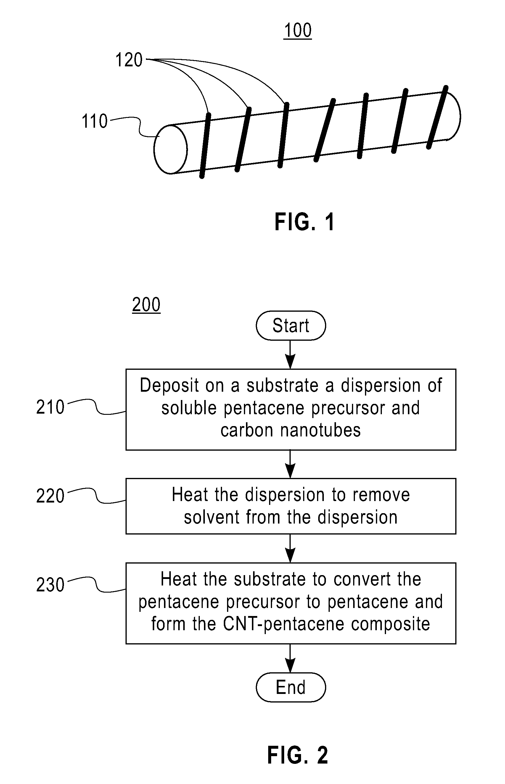
[0048]The dispersion of pentacene precursors and carbon nanotubes may be deposited (e.g., by spin coating, drop cast, etc.) on the insulation layer 404 (e.g., between the source and drain electrodes 406, 408). The solvent is removed (e.g., by heating at low temperature such as in a ra...


PUM

PropertyMeasurementUnit
temperatureaaaaaaaaaa
charge carrier mobilityaaaaaaaaaa

Abstract

A composite material includes a carbon nanotube, and plural pentacene molecules bonded to the carbon nanotube. A method of forming the composite layer, includes depositing on a substrate a dispersion of soluble pentacene precursor and carbon nanotubes, heating the dispersion to remove solvent from the dispersion, heating the substrate to convert the pentacene precursor to pentacene and form the carbon nanotube-pentacene composite layer.

Description

BACKGROUND OF THE INVENTION[0001]1. Field of the Invention[0002]The present invention relates to a composite material which includes a carbon nanotube, and plural pentacene molecules bonded to the carbon nanotube, and more particularly, to a method of forming a semiconductor device including forming a channel region which includes a carbon nanotube-pentacene composite layer.[0003]2. Description of the Related Art[0004]Organic semiconductors have been studied extensively for use as channel materials in thin film transistors. In particular, solution processed pentacene thin film transistors (TFT) have been formed using soluble pentacene precursors which after deposition on the surface could be converted to pentacene by moderate heating. For example, see U.S. Pat. No. 6,963,080 to Afzali-Ardakani et al. entitled “THIN FILM TRANSISTORS USING SOLUTION PROCESSED PENTACENE PRECURSOR AS ORGANIC SEMICONDUCTOR”, and U.S. Pat. No. 7,125,989 to Afzali-Ardakani et al. entitled “HETERO DIELS-ALDE...

Claims


Application Information

Patent Timeline
Patent Type & Authority Patents(United States)
IPC IPC(8): H01L29/08H01L51/00H01L35/24
CPCB82Y10/00B82Y30/00B82Y40/00C01B31/0273C07C15/20H01L51/0049H01L51/0055C01B2202/02C01B2202/22C01P2004/13C01P2004/133C01P2004/61C07C2103/52H01L51/0003H01L51/0541H01L51/0545Y02E10/549C07C2603/52C01B32/174H10K71/12H10K85/225H10K85/623H10K10/464H10K10/466
Inventor AFZALI-ARDAKANI, ALIKAGAN, CHERIE R.TROMP, RUDOLF M.
Owner GLOBALFOUNDRIES U S INC
Why Eureka
Try Eureka