Method for fabricating semiconductor device

a semiconductor device and forming technology, applied in semiconductor devices, semiconductor/solid-state device details, electrical devices, etc., can solve the problems of poor contact between the bit line and the bit line contact, and achieve the effect of preventing the resistance from being increased, and increasing the width of the bit lin

Active Publication Date: 2013-11-12
SK HYNIX INC
View PDF17 Cites 1 Cited by
  • Summary
  • Abstract
  • Description
  • Claims
  • Application Information

AI Technical Summary

Benefits of technology

[0007]An object of the present invention is to provide a semiconductor device having a buried gate, which prevents the occurrence of poor contact between a bit line and a bit line contact during the patterning of a bit line, and also prevents resistance from being increased when patterning is performed to increase the width of a bit line. That is, the semiconductor device can solve the problems of the related art. The problems of the related art are as follows. According to the related art, if a bit line is reduced in width and a bit line is misaligned during the patterning of a bit line, a bit line contact coupled to the bottom of the bit line is exposed so that there arises poor contact between the bit line and the bit line contact. In addition, according to the related art, if the patterning is performed in such a manner that the width of bit line is increased, a coupling width of a storage electrode contact formed in a subsequent process becomes narrower, resulting in increased resistance.

Problems solved by technology

According to the related art, if a bit line is reduced in width and a bit line is misaligned during the patterning of a bit line, a bit line contact coupled to the bottom of the bit line is exposed so that there arises poor contact between the bit line and the bit line contact.

Method used


Image

  • Method for fabricating semiconductor device
  • Method for fabricating semiconductor device
  • Method for fabricating semiconductor device

Examples


Embodiment Construction

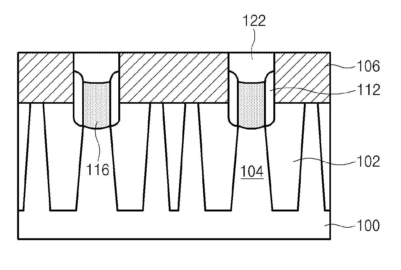
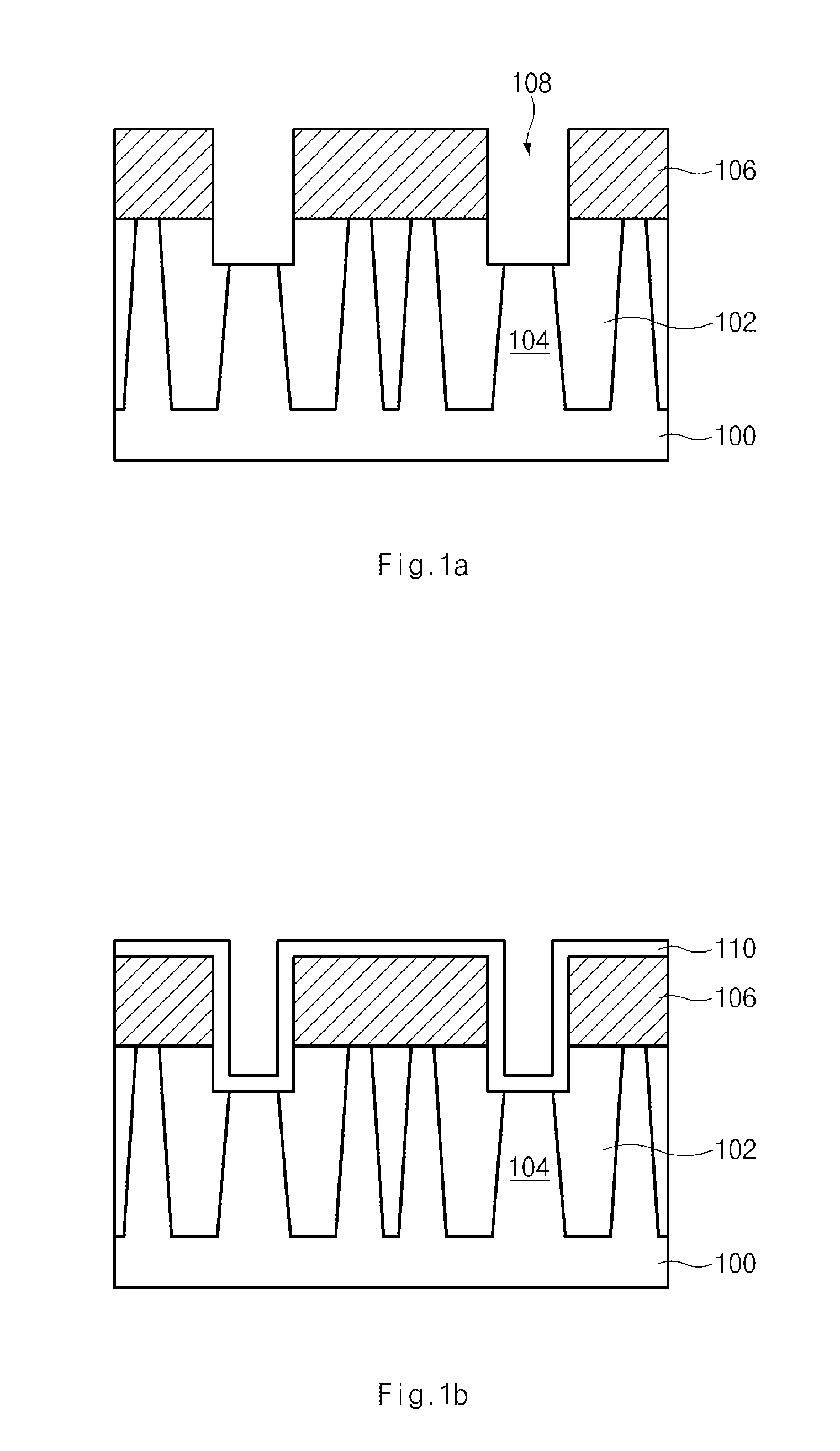
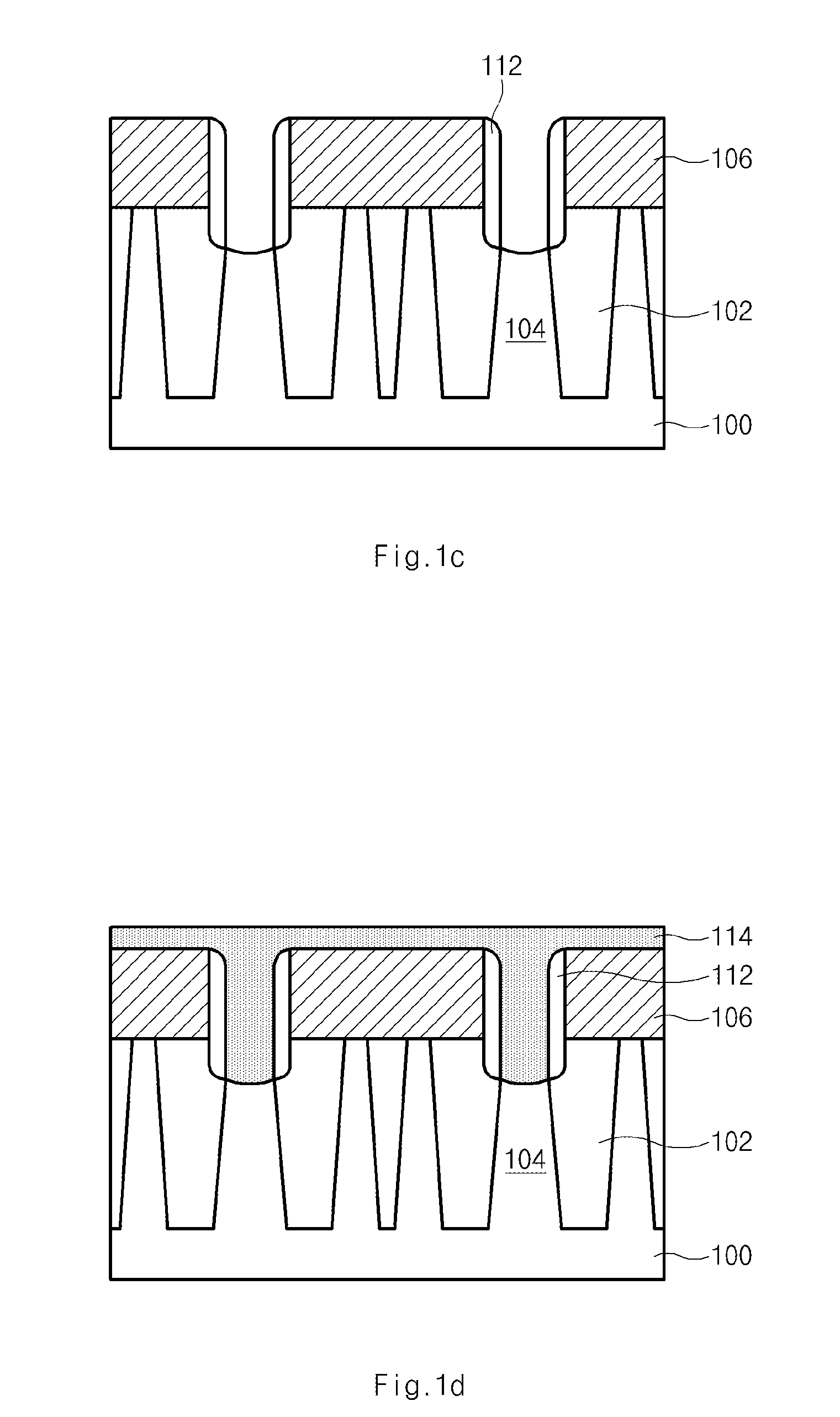
[0030]Reference will now be made in detail to the embodiments of the present invention, examples of which are illustrated in the accompanying drawings. Wherever possible, the same reference numbers will be used throughout the drawings to refer to the same or like parts.

[0031]FIGS. 1A to 1J are cross-sectional views illustrating a method for forming a semiconductor device according to one embodiment of the present invention. FIGS. 1K to 1L are cross-sectional views illustrating a method for forming a semiconductor device according to another embodiment of the present invention.

[0032]Referring to FIG. 1A, an interlayer insulating film 106 is formed over the semiconductor substrate 100 including an active region 104 defined by a device isolation film 102. Although not shown in FIG. 1A, it is preferable that the semiconductor substrate 100 includes a buried gate. Subsequently, the interlayer insulating film 106 is etched to expose the active region 104, so that a bit line contact hole 1...


PUM


Abstract

A method for forming a semiconductor device is disclosed. A method for forming a semiconductor device includes forming a first bit line contact over a semiconductor substrate, forming a second bit line contact that is coupled to the first bit line contact and has a larger width than the first bit line contact, and forming a bit line over the second bit line contact. When using the semiconductor device having a buried gate, although the bit line is formed to have a small width and the bit line pattern is misaligned, the method prevents incorrect coupling between a bit line and a bit line contact, so that it basically deteriorates unique characteristics of the semiconductor device.

Description

CROSS-REFERENCE TO RELATED APPLICATION[0001]The present application claims priority to Korean patent application number 10-2010-0001660, filed on 8 Jan. 2010, which is incorporated by reference in its entirety.BACKGROUND OF THE INVENTION[0002]Embodiments of the present invention relate to a method for forming a semiconductor device, and more particularly to a method for forming a bit line in a semiconductor device including a buried gate.[0003]Among semiconductor memory devices, a dynamic random access memory (DRAM) device includes a plurality of unit cells each having a capacitor and a transistor. The capacitor is used to temporarily store data, and the transistor is used to transfer data between a bit line and the capacitor in response to a control signal applied through a word line. The data transfer occurs by using a semiconductor property where an electrical conductivity changes depending on environments. The transistor has three regions, i.e., a gate, a source, and a drain. El...

Claims


Application Information

Patent Timeline
Patent Type & Authority Patents(United States)
IPC IPC(8): H01L21/44
CPCH01L27/10888H01L29/41766H01L23/48H01L21/76831H01L2924/0002H01L2924/00H10B12/485
Inventor KIM, HYUN JUNG
Owner SK HYNIX INC
Why Eureka
Try Eureka