Phase noise tolerant sampling

Active Publication Date: 2013-10-15
ANALOG DEVICES INT UNLTD
View PDF11 Cites 31 Cited by
  • Summary
  • Abstract
  • Description
  • Claims
  • Application Information

AI Technical Summary

Benefits of technology

The patent describes a solution to problems with measuring phase noise in clock signals. The invention provides a way to sample signals that are more tolerant to phase noise, making it easier to use in electronic devices.

Problems solved by technology

Phase noise, on the other hand, may be considerable because the phase noise has no such mechanism to restore the phase to ideal in the face of disturbances except the PLL.
When the phase-locked loop VCO is used to drive mixer switches of a radio mixer or initiate a sampling operation in an analog-to-digital converter (ADC), the phase noise causes timing jitter.
Timing jitter results in a decrease in the output-signal fidelity because the jitter causes the desired signal to be modulated, thereby converting a portion of the desired energy into noise.
This noise has the effect of increasing the error vector magnitude (EVM) of the symbol constellation generated at the mixer outputs from the I / Q demodulated data, since phase noise causes the orthogonal basis functions to deviate from a constant rotation rate.
Similar deleterious behaviors are observed in sampling of a signal by a stand-alone ADC.
The design choice of using an inductor for the VCO comes with the additional disadvantage that a large amount of power must be consumed by the VCO to maintain oscillation at the desired energy / loss ratio.
Furthermore, use of an inductor-based VCO exposes the device to susceptibility to electromagnetic interference from external sources, such as an on-board or on-chip DCDC converter comprising an inductor.
Note, however, that the phase noise of the ring oscillator is substantially higher than the phase noise of the LC oscillator.
Both of these choices cause dramatic increase in power consumption.
Finally, in some embodiments even the use of an inductor-based VCO yields inadequate phase noise performance.
However, phase noise will cause the ADC output to vary from desired based upon the timing jitter and the signal ramp rate.
Phase noise may cause mixing of adjacent channels into the desired sampling bandwidth.

Method used


Image

  • Phase noise tolerant sampling
  • Phase noise tolerant sampling
  • Phase noise tolerant sampling

Examples


Embodiment Construction

[0035]In the following detailed description, numerous specific details are set forth by way of examples in order to provide a thorough understanding of the relevant teachings. However, it should be apparent to those skilled in the art that the present teachings may be practiced without such details. In other instances, well known methods, procedures, components, and / or circuitry have been described at a relatively high-level, without detail, in order to avoid unnecessarily obscuring aspects of the present teachings.

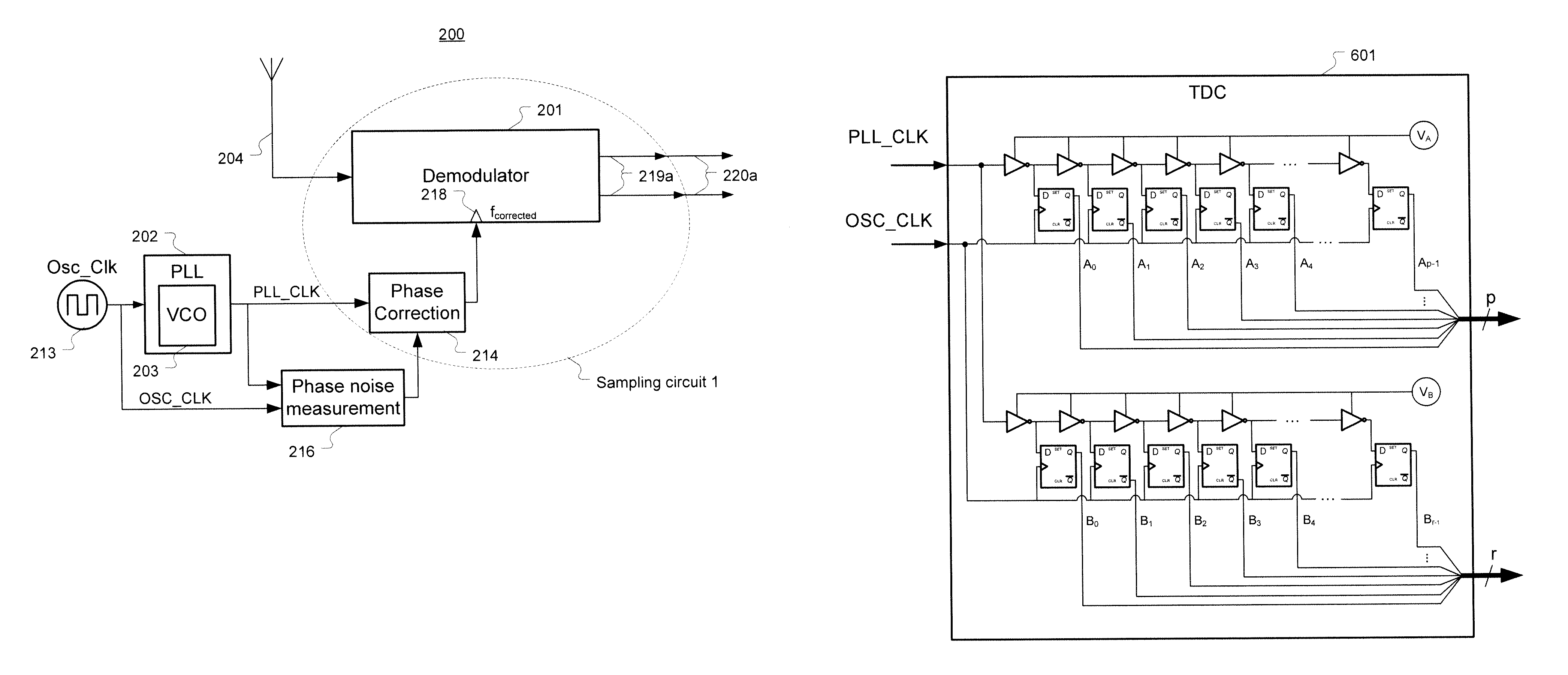
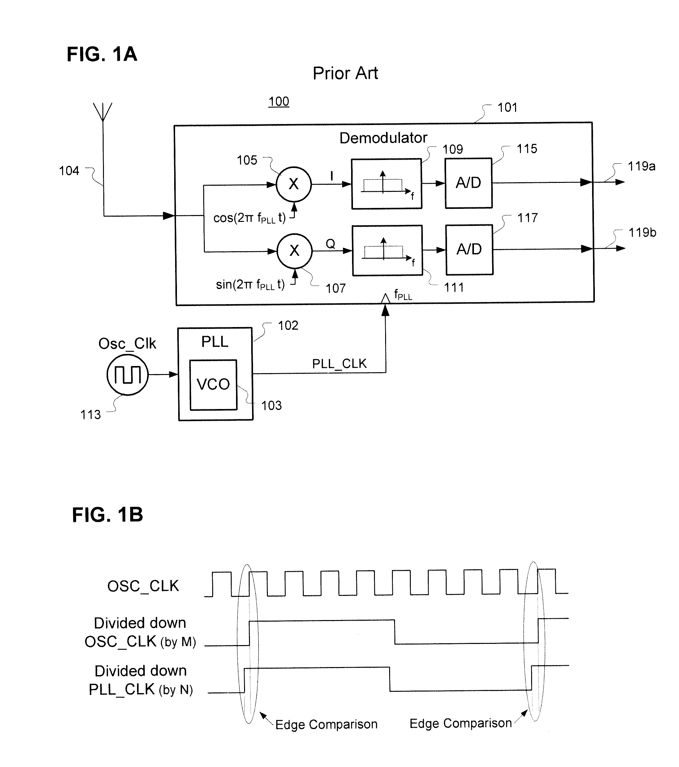
[0036]The various systems and methods disclosed herein relate to the measurement of phase noise or jitter between a reference clock signal provided by an oscillator and a PLL clock signal at an output of a PLL / VCO, and the provision of a corrected timing reference signal or the correction of a sampled signal using the measured phase noise.

[0037]Reference now is made in detail to the examples illustrated in the accompanying drawings and discussed below. The systems and met...


PUM


Abstract

Phase noise in a first clock signal is measured using a time to digital converter (TDC) by determining variations in the phase delay between the first clock signal and a second clock signal. The TDC can include first and second series interconnections of delay elements, first and second sets of latches, and processing circuitry coupled to the latches and configured to determine the phase delay. The TDC can include a series interconnection of delay elements, latches, and circuitry configured to selectively adjust the control signal connected to the delay elements based on the output of the latches. The phase noise measurement can be used in a sampling circuit, so as to produce a second data signal from a first data signal based on the first clock signal and the measured phase noise.

Description

FIELD OF THE INVENTION[0001]The present subject matter relates to techniques and equipment to measure phase noise in a clock signal, and to provide phase-noise tolerant sampling by removing the measured phase noise from the clock signal used for sampling, or by correcting a sampled signal using the measured phase noise.BACKGROUND[0002]A modem radio receiver, such as the radio receiver 100 shown in FIG. 1A, includes a demodulator 101 which utilizes a phase-locked loop (PLL) 102 including a voltage controlled oscillator (VCO) 103 to demodulate an analog RF input signal received at antenna 104 by projecting the RF input signal onto a rotating orthogonal basis comprising an in-phase (I) and a quadrature-phase (Q) coordinate system. Projection is accomplished by first multiplying, using a multiplier 105, the incoming signal by the local oscillator signal cos(2π·fPLL·t) to obtain the in-phase component I of the RF signal, and filtering the resulting signal using a low-pass filter 109. Sim...

Claims


Application Information

Patent Timeline
IPC IPC(8): H03M1/50
CPCG01R31/31709H03L7/08H03L7/18
Inventor LEMKIN, MARK ALANJUNEAU, THOR NELSON
Owner ANALOG DEVICES INT UNLTD
Why Eureka
Try Eureka