Eureka AIR delivers breakthrough ideas for toughest innovation challenges, trusted by R&D personnel around the world.

Multi-cavity vacuum electron beam device for operating at terahertz frequencies

a vacuum electron beam and terahertz frequency technology, applied in the direction of discharge tube/lamp details, amplifiers with transit-time effect, discharge tube luminescnet screens, etc., can solve the problems of high-order multipliers that are inefficient, require millions of dollars of investment, and are very expensiv

Active Publication Date: 2013-05-14
LOGOS TECH HOLDCO INC
View PDF6 Cites 9 Cited by
  • Summary
  • Abstract
  • Description
  • Claims
  • Application Information

AI Technical Summary

Problems solved by technology

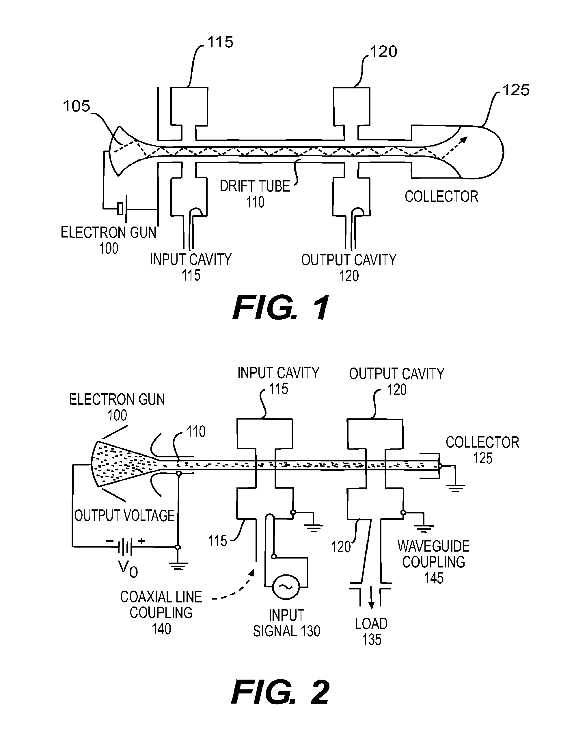
Despite the obvious potential of THz radiation, sources of T-rays remain either very expensive, very low power, or both.
High order multipliers are inefficient, so many THz sources use stacked low order frequency multipliers.
While this yields high power radiation, it requires millions of dollars of investment, and a large facility, of which only a handful exist in the world.
Solid state signal sources are limited by material properties at high frequencies, and therefore have difficulties exceeding 100 GHz.
It ultimately failed under test due to a magnetic misalignment.
The individual cavities are on the order of 1 mm, but the tolerance is <0.2%, to attain the required Q. LIGA seems to have a lot of potential; however it is limited in its use, because it requires a hard x-ray source for exposure, such as a synchrotron, and long exposure times (4-8 hours).
As such, waiting lists for LIGA exposure are months or even years long.
Several proposals have been produced, and various components have been fabricated, however no functional device has been produced.
While Manohora and his colleagues at the Jet Propulsion Lab propose using a carbon nanotube field emission array (FEA), they have not succeeded in creating such a device.
Backward wave oscillators offer more tunability than klystrons, but give up efficiency.
The structure has been fabricated using LIGA, however only 8% of the fabricated circuits were in usable condition.
The resonant structure has been fabricated, but successful operation has not yet been demonstrated.

Method used


Image

  • Multi-cavity vacuum electron beam device for operating at terahertz frequencies
  • Multi-cavity vacuum electron beam device for operating at terahertz frequencies
  • Multi-cavity vacuum electron beam device for operating at terahertz frequencies

Examples


examples

[0085]In accordance with certain embodiments of the invention, exemplary devices were prepared and evaluated.

example a

See FIGS. 36a-36e

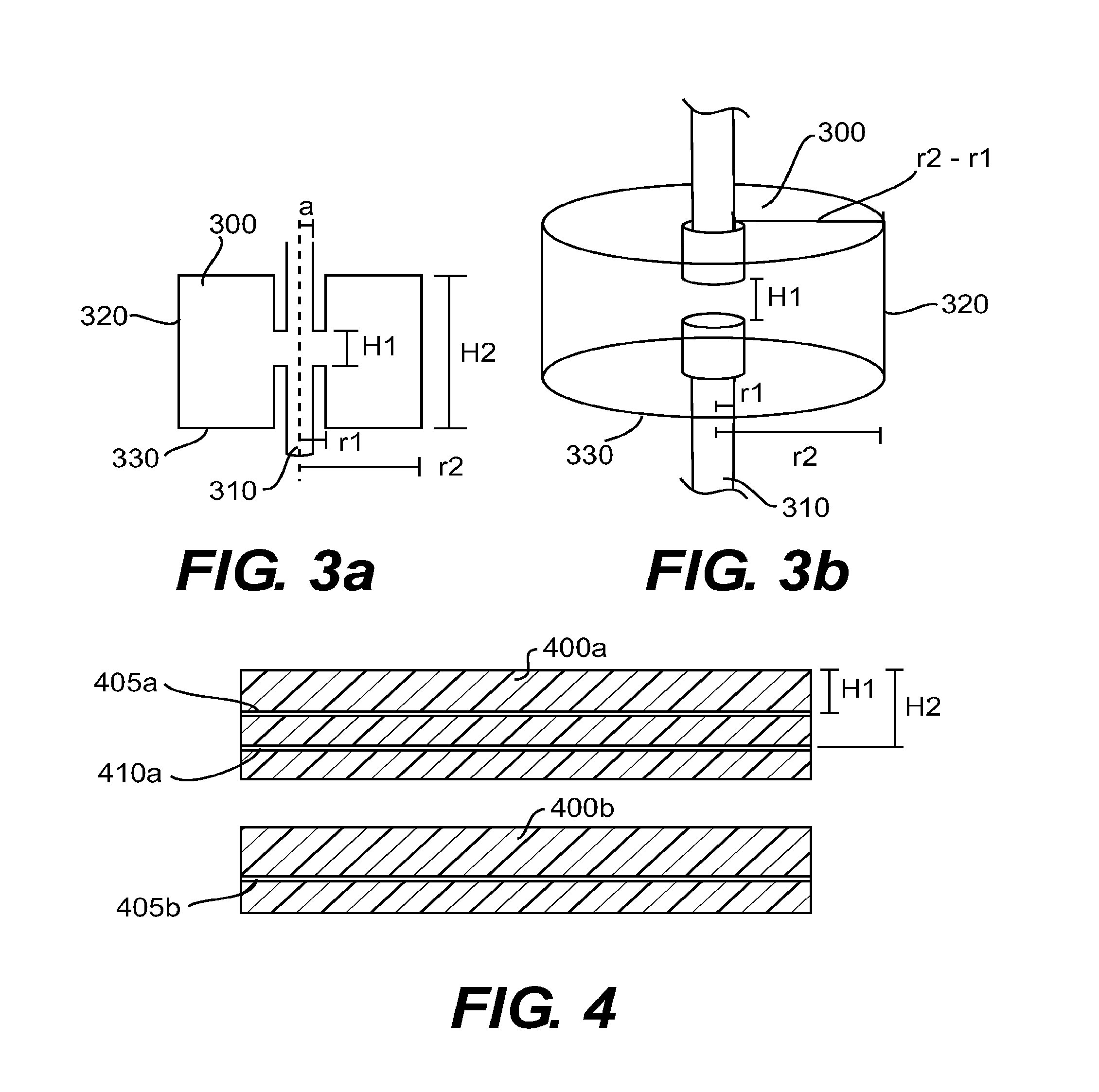
[0086]A THz emitter array Klystron was fabricated, as generally illustrated in FIGS. 36a-36f. As shown on FIG. 36a, each resonant cavity was fabricated to have the following dimensions.

[0087]

Dimension ValueH1100 umH2430 umr135 umr2400 uma35 um

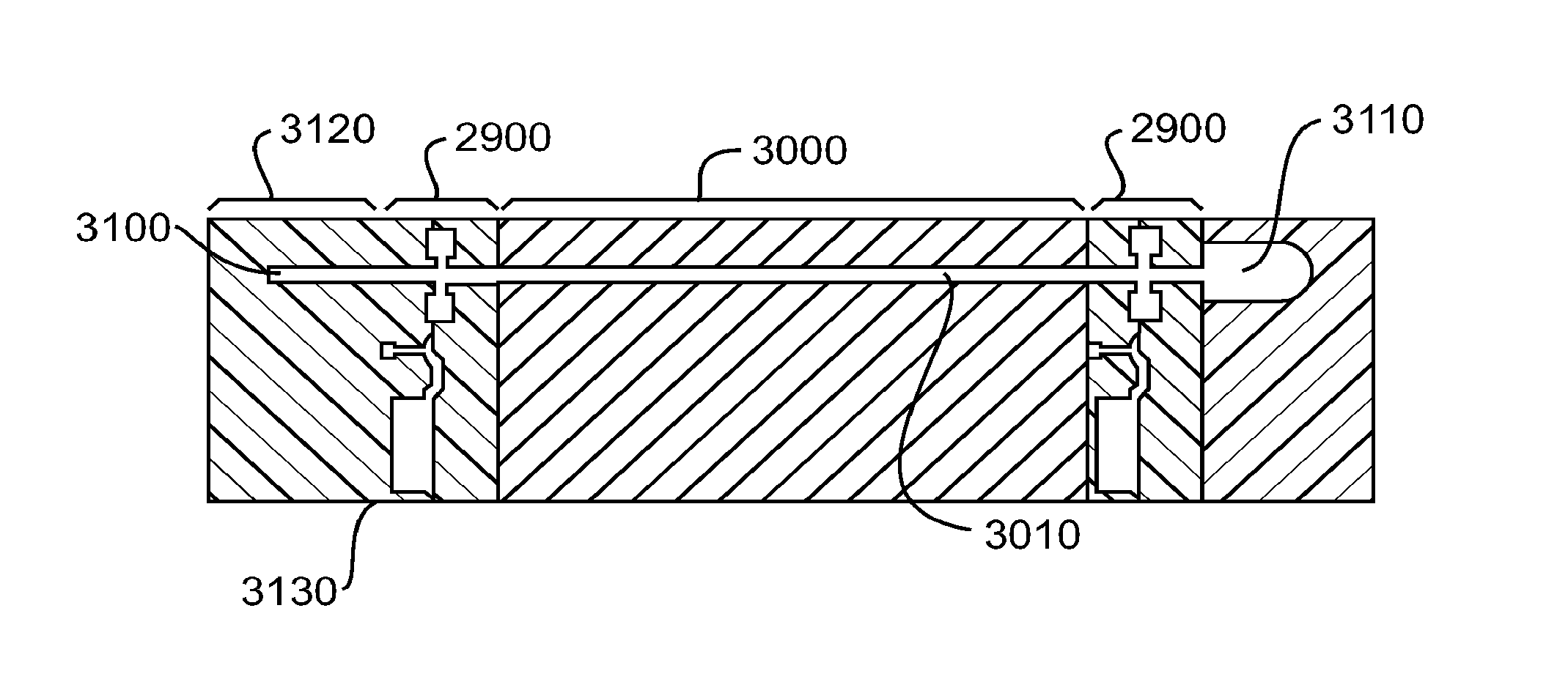
[0088]The fabrication methods utilized DRIE etching and wafer-level (or die-level) fusion bonding of silicon wafers to form a negative mold that was coated with sputtered or electrodeposited copper. As shown on FIG. 36b, in one embodiment, an 8 kV gun voltage ‘stock’ FEA 100 with a current density of 40 A / cm2 was fusion-bonded to the base of the tube stack 110 (with a dielectric spacer 3600 between the tube stack 110 and the electron gun 100 having a 1 MV / m field gradient), with the electron beam 105 diameter confined by a 1T magnetic field generated by two permanent magnets 3610 and aligned with the axis of the tube 110. The fabrication process provided excellent alignment of the magnetic field with the tube axis, and allowed...

example b

[0092]A 2-cavity klystron was prepared according to fabrication methods of the invention. The beam tunnel diameter for both current, and cavity coupling was optimized while making some reasonable assumptions about current density and filling factor results in a beam tunnel radius of 35 μm, and a beam radius of 25 μm. To obtain such a fine beam with a conventional thermionic cathode would require beam shaving, which would significantly lower the tube efficiency. The alternate approach is to use a FEA, which can produce the necessary current density without beam compression. This also allows for easy integration with a micro-fabricated tube, and simplifies the magnetic field design.

[0093]FEAs are capable of producing very high current densities, often exceeding several hundred A / cm2 in ideal conditions. A vacuum tube environment provides less than ideal conditions for an FEA, however it does seem reasonable to expect current densities up to 40 A / cm2. Additionally, FEA performance impr...


PUM


Abstract

The present invention relates to the formation of a vacuum electronics circuit by the fusion bonding of multiple substrate wafers, e.g., silicon, copper, or other suitable conductive material, each etched using DRIE, cut using EDM, or machined by other suitable means. Other aspects of the invention relate to the alignment of a cathode with tube by fusion bonding the cathode wafer to a tube built using the fabrication methods described herein. Yet other aspects involve the alignment of dies or wafers during the fabrication of a vacuum electronics device using the “lego” technique outlined herein. In yet other aspects, fabrication methods are described.

Description

RELATED APPLICATIONS[0001]The present application claims the benefit of U.S. Provisional Application No. 61 / 053,577, filed May 15, 2008, the entire contents of which are herein incorporated by reference in its entirety.FIELD OF THE INVENTION[0002]The present invention relates generally to devices for generating electromagnetic radiation. More particularly, embodiments of the present invention include vacuum electronic devices and resonant cavities for use in such devices, and methods of micro-fabricating such devices and cavities.BACKGROUND OF THE INVENTION[0003]The Radio Frequency (RF) spectrum extends from low frequency radio, through radio, microwave, terahertz, infra-red, visible, ultra-violet, and finally x-rays, and while the fundamental form of all the waves are the same, the mechanism for formation, and absorption of each varies. Radio and microwaves are created by macroscopic currents flowing or oscillating through a bulk material—as in a semiconductor, or and antenna. Much...

Claims


Application Information

Patent Timeline
Patent Type & Authority Patents(United States)
IPC IPC(8): H01J25/10
CPCH01J25/10
Inventor PROTZ, JONATHAN MICHAELVERDIEL, MARC STEPHENFIELDS, DAVID JAMES
Owner LOGOS TECH HOLDCO INC
Why Eureka
Eureka Blog
Learn More