Bulk sulfide species treatment of thin film photovoltaic cell and manufacturing method

Inactive Publication Date: 2013-05-07
CM MFG
View PDF240 Cites 3 Cited by
  • Summary
  • Abstract
  • Description
  • Claims
  • Application Information

AI Technical Summary

Benefits of technology

The patent text describes a thin film photovoltaic device that includes a substrate with a surface region, a first electrode layer, and a layer of chalcopyrite material. The chalcopyrite material consists of a copper poor copper indium disulfide bulk region and a surface region. To improve the device's performance, a compensating sodium species is added to change the copper poor copper indium disulfide region from an n-type impurity characteristic to a p-type impurity characteristic. Additionally, a compensating sulfur species is added to provide a desirable conversion efficiency characteristic for the device. The device also includes a window layer and a second electrode layer. The technical effects of this patent are improved performance and efficiency of thin film photovoltaic devices.

Problems solved by technology

Unfortunately, the supply of petrochemical fuel is limited and essentially fixed based upon the amount available on the planet Earth.
Additionally, as more people use petroleum products in growing amounts, it is rapidly becoming a scarce resource, which will eventually become depleted over time.
Although solar energy is environmentally clean and has been successful to a point, many limitations remain to be resolved before it becomes widely used throughout the world.
However, crystalline materials are often costly and difficult to make on a large scale.
Additionally, devices made from such crystalline materials often have low energy conversion efficiencies.
Similar limitations exist with the use of thin film technology in making solar cells.
That is, efficiencies are often poor.
Additionally, film reliability is often poor and cannot be used for extensive periods of time in conventional environmental applications.
Often, thin films are difficult to mechanically integrate with each other.

Method used


Image

  • Bulk sulfide species treatment of thin film photovoltaic cell and manufacturing method
  • Bulk sulfide species treatment of thin film photovoltaic cell and manufacturing method
  • Bulk sulfide species treatment of thin film photovoltaic cell and manufacturing method

Examples


Embodiment Construction

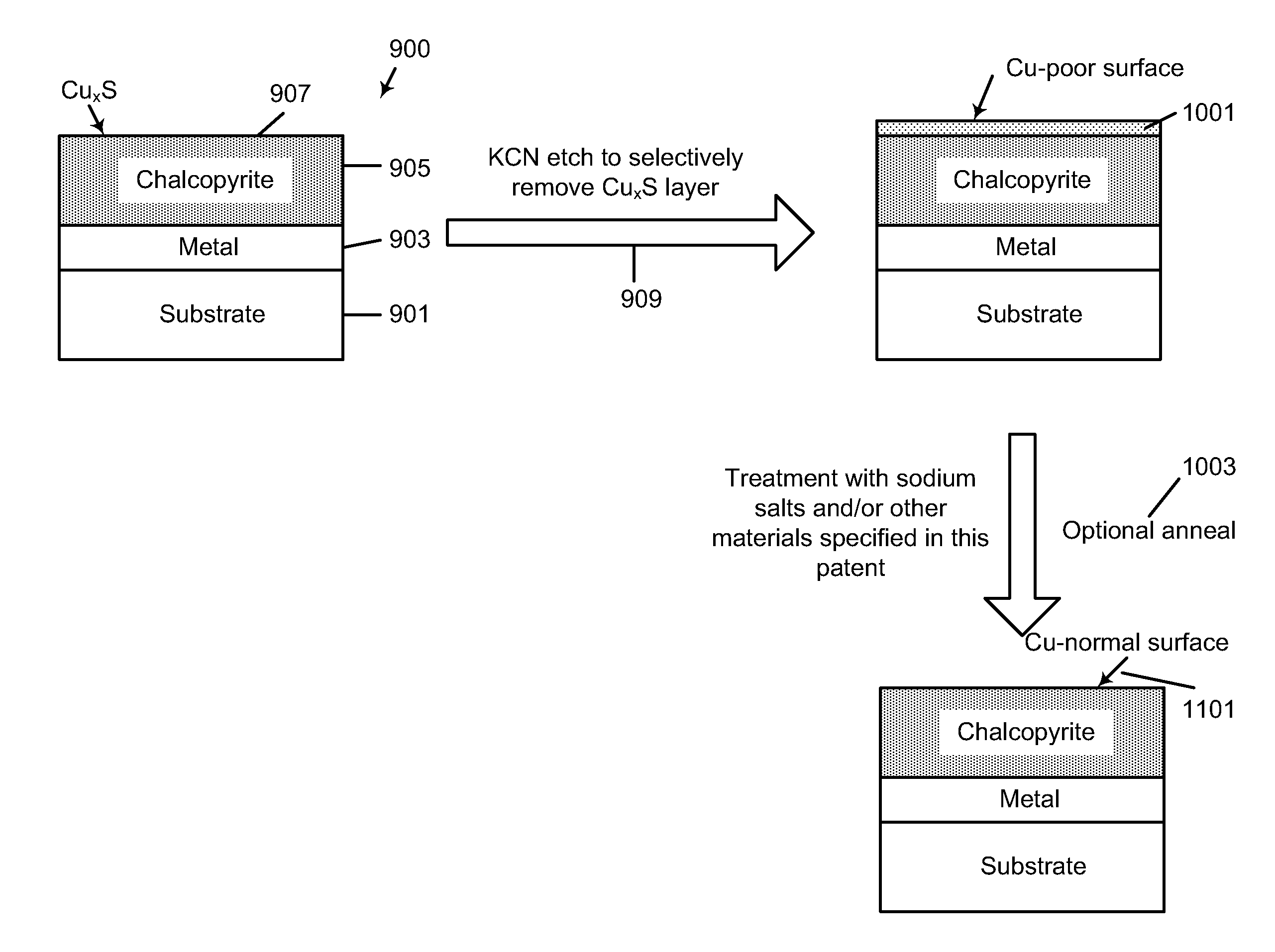
[0019]According to embodiments of the present invention, a method and a structure for forming semiconductor materials for photovoltaic applications are provided. More particularly, the present invention provides a method for manufacturing thin film photovoltaic devices. Merely by way of example, the method has been used to provide a copper indium disulfide thin film material for high efficiency solar cell application. But it would be recognized that the present invention has a much broader range of applicability, for example, embodiments of the present invention may be used to form other semiconducting thin films or multi layers comprising iron sulfide, cadmium sulfide, zinc selenide, and others, and metal oxides such as zinc oxide, iron oxide, copper oxide, and others.

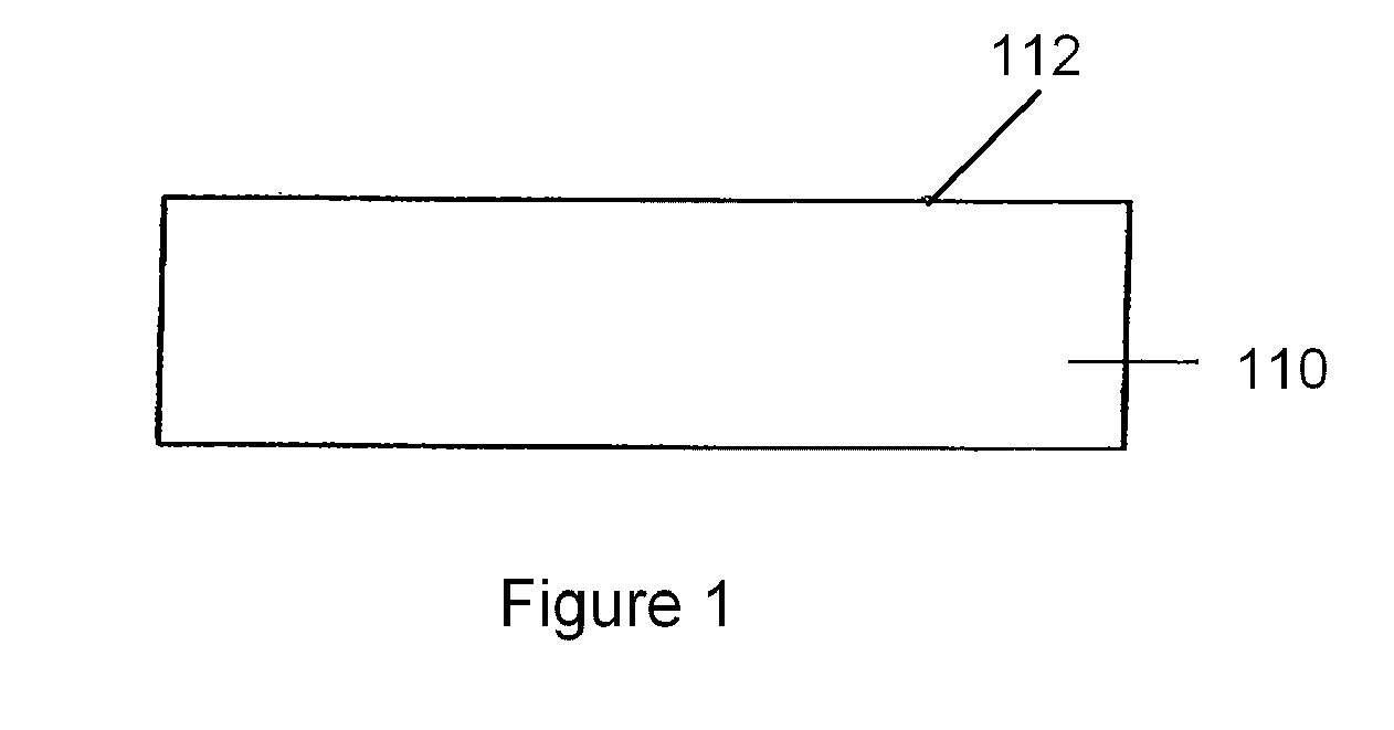
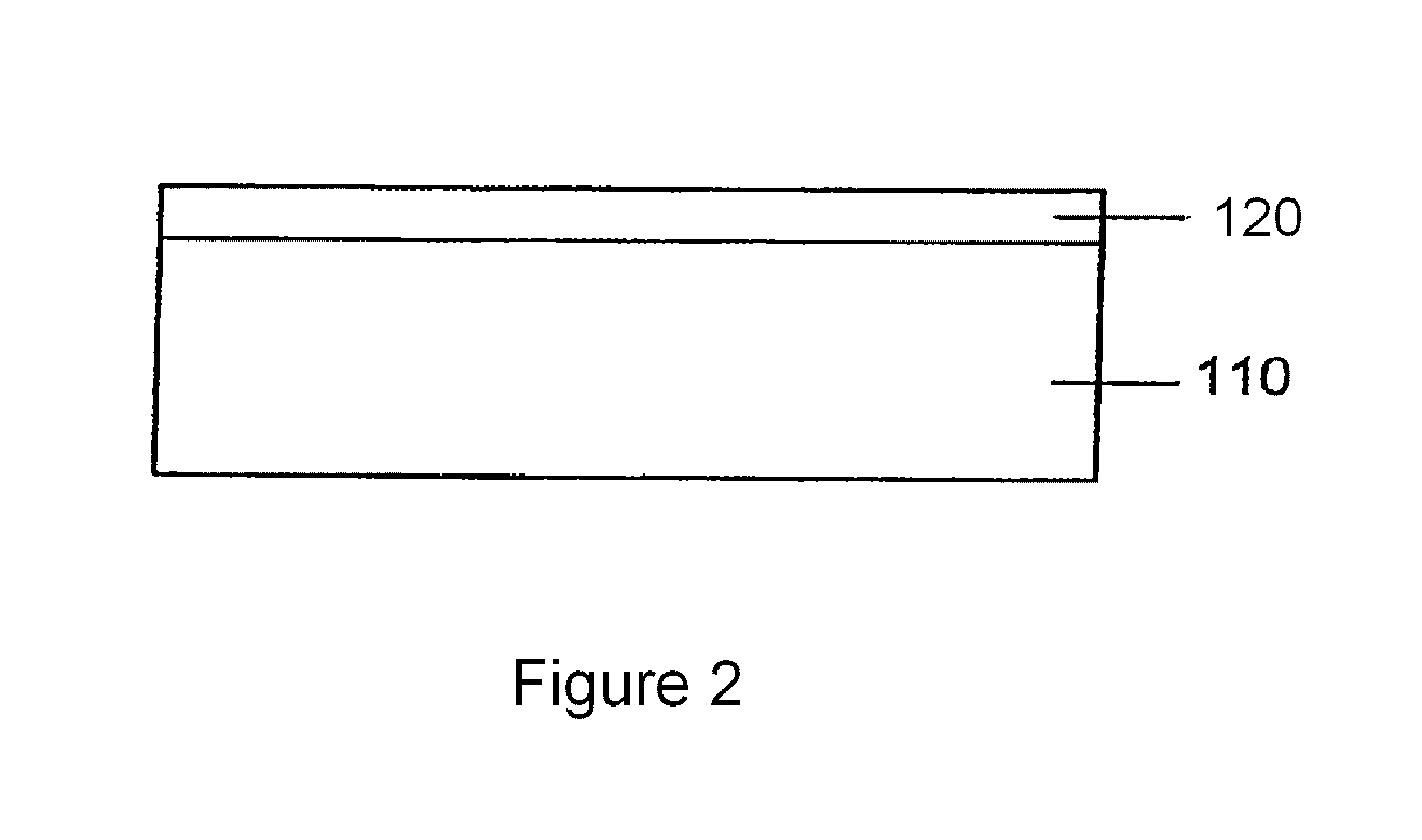
[0020]FIGS. 1-8 are simplified schematic diagrams illustrating a method for forming a thin film photovoltaic device according to an embodiment of the present invention. These diagrams are merely examples, which should...


PUM


Abstract

A method for forming a thin film photovoltaic device. The method includes providing a transparent substrate comprising a surface region and forming a first electrode layer overlying the surface region. The method forms a bulk copper indium disulfide material from a multi-layered structure comprising a copper species, an indium species, and a sulfur species overlying the first electrode layer. The bulk copper indium disulfide material comprises one or more portions of a copper poor copper indium disulfide material, a copper poor surface regions, and one or more portions of a sulfur deficient copper indium disulfide material characterized by at least a CuInS2-x species, where 0<x<2. The copper poor surface and one or more portions of the copper poor copper indium disulfide material are subjected to a sodium species derived from a sodium sulfide material to convert the copper poor surface from an n-type characteristic to a p-type characteristic. The method also subjects the one or more portions of the sulfur deficient copper indium disulfide material to a sulfur species derived form the sodium sulfide material to improve a conversion efficiency characteristic of the photovoltaic device. A window layer is formed overlying the copper indium disulfide material.

Description

CROSS-REFERENCES TO RELATED APPLICATIONS[0001]This application claims priority to U.S. Provisional Patent Application No. 61 / 103,549 filed Oct. 7, 2008, entitled “BULK SULFIDE SPECIES TREATMENT OF THIN FILM PHOTOVOLTAIC CELL AND MANUFACTURING METHOD” by inventor HOWARD W. H. LEE, commonly assigned and incorporated by reference herein for all purposes. This application is related to U.S. Provisional Patent Application No. 61 / 103,239 filed Oct. 6, 2008, commonly assigned and incorporated by reference herein for all purposes. This application is also related to U.S. patent application Ser. No. 12 / 567,715 filed Sep. 25, 2009, now U.S. Pat. No. 8,003,430, commonly assigned and incorporated by reference herein for all purposes.BACKGROUND OF THE INVENTION[0002]The present invention relates generally to photovoltaic materials and manufacturing method. More particularly, the present invention provides a method and structure for manufacture of high efficiency thin film photovoltaic cells. Mer...

Claims


Application Information

Patent Timeline
IPC IPC(8): H01L21/38
CPCH01L31/0749H01L31/0322Y02E10/541
Inventor LEE, HOWARD W. H.
Owner CM MFG
Why Eureka
Try Eureka