
Cavity-free interface between extension regions and embedded silicon-carbon alloy source/drain regions

a technology of extension region and embedded silicon, which is applied in the field of field-effect transistors, can solve the problems of limited deposition of doped silicon-carbon alloy, failure to use n-doped silicon-carbon alloy, and formation of cavities, and achieve the effect of enhancing the mobility of electrons

Active Publication Date: 2013-03-12
GLOBALFOUNDRIES U S INC
View PDF16 Cites 7 Cited by
  • Summary
  • Abstract
  • Description
  • Claims
  • Application Information

AI Technical Summary

Benefits of technology

This approach eliminates cavity formation, enhancing the contact resistance between source / drain extension regions and embedded source / drain regions, thereby improving the on-current and mobility of electrons in transistors.

Problems solved by technology

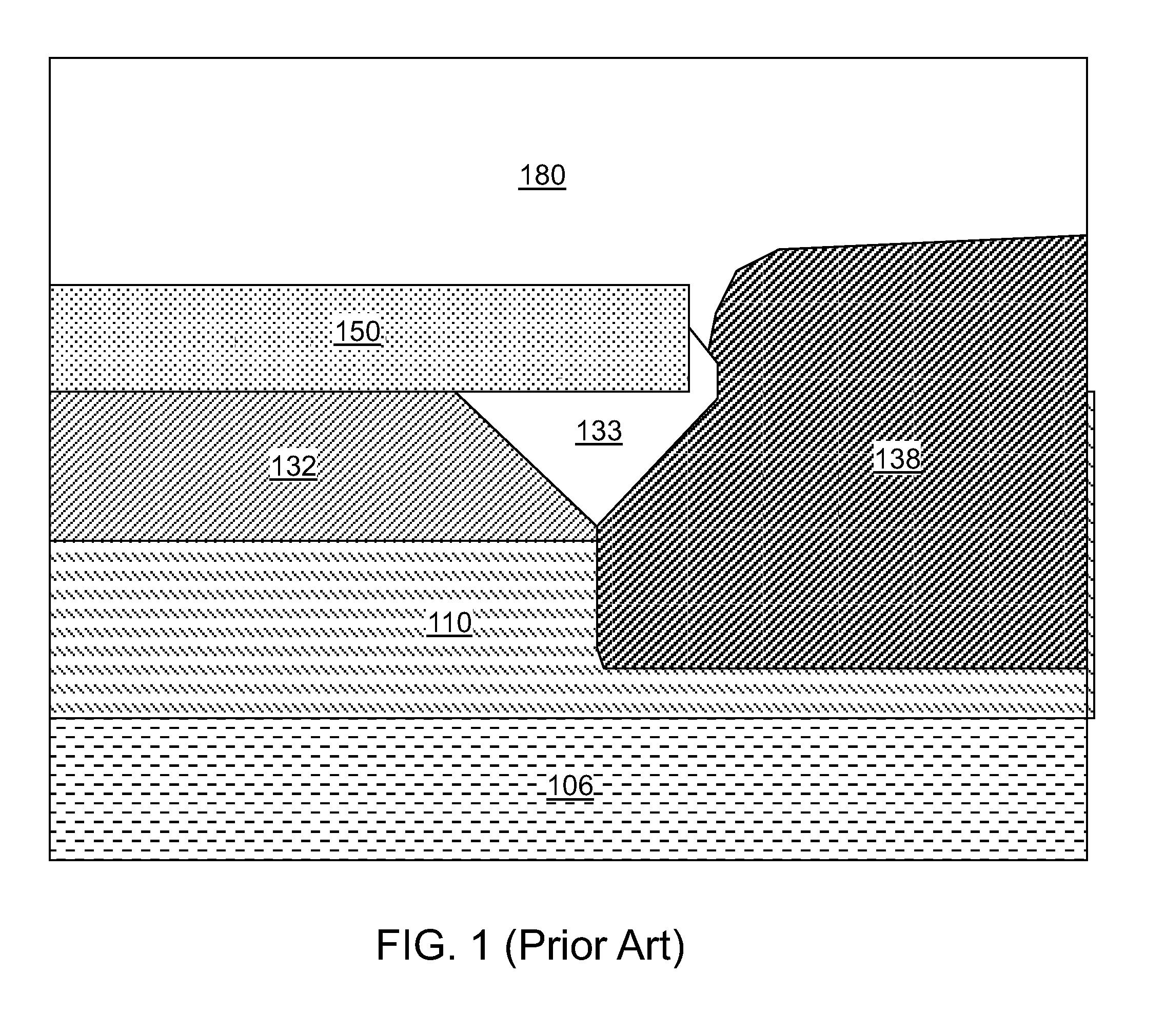
Experimentally, attempts to use an n-doped silicon-carbon alloy for embedded source / drain regions encounters a practical problem of cavity formation at an interface between preexisting source / drain extension regions and epitaxially grown N-type Silicon-Carbon.
In prior art structures, deposition of the doped silicon-carbon alloy is limited by the supply of reactant gases into a geometry having a high aspect ratio at the interfaces between source / drain extension regions and the dielectric gate spacers.
This local imbalance between the deposition rate and the etch rate induces formation of cavities during attempted selective epitaxy processes for depositing a silicon-carbon alloy.
These cavities penalize the link-up resistance between extension and epitaxial source / drain regions causing a undesired resistance increase in the transistor.
Such cavities, when formed at an interface between a source / drain extension region and an embedded doped silicon-carbon alloy portion, have a deleterious effect on the performance of the field effect transistors because the resistance between an embedded doped silicon-carbon alloy portion, which function as a source / drain region, and the source / drain extension regions adjacent to the embedded doped silicon-carbon alloy portion increase with the size of the cavities.

Method used


Image

  • Cavity-free interface between extension regions and embedded silicon-carbon alloy source/drain regions
  • Cavity-free interface between extension regions and embedded silicon-carbon alloy source/drain regions
  • Cavity-free interface between extension regions and embedded silicon-carbon alloy source/drain regions

Examples


Embodiment Construction

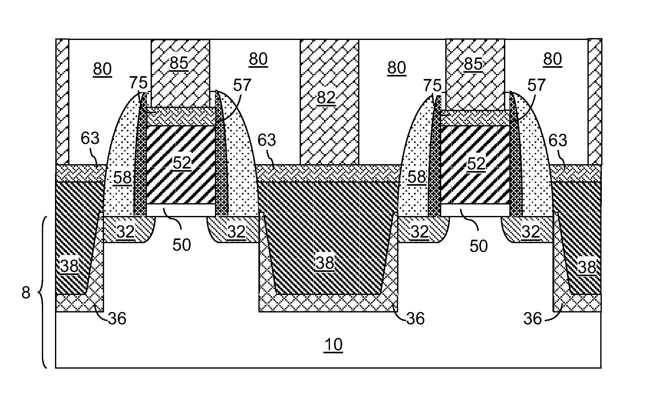
[0019]As stated above, the present disclosure relates to field effect transistors including an embedded source / drain region having an n-doped silicon liner and an n-doped silicon-carbon alloy interior portion, and methods of manufacturing the same, which are now described in detail with accompanying figures. It is noted that like reference numerals refer to like elements across different embodiments. The drawings are not necessarily drawn to scale.

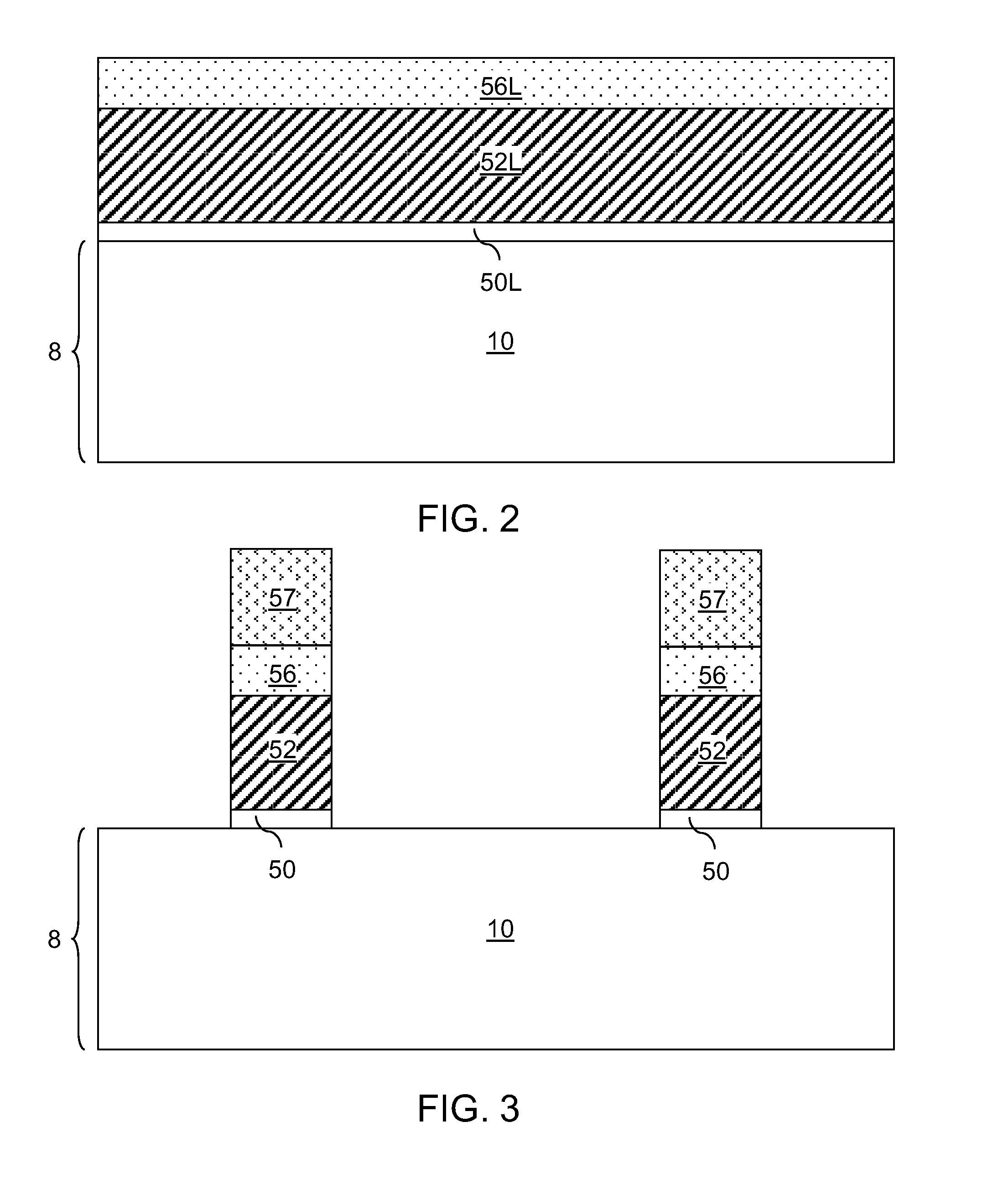
[0020]Referring FIG. 2, an exemplary semiconductor structure according to an embodiment of the present disclosure includes a semiconductor substrate 8, which is a single crystalline silicon substrate layer 10 having a p-type doping. Thus, the single crystalline silicon substrate layer 10 consists essentially of silicon and p-type dopants. The p-type dopants included in the single crystalline silicon substrate layer 10 can be, for example, B, Ga, In, Tl, or a combination thereof. The concentration of the p-type dopants in the single crystal...


PUM


Abstract

A gate stack is formed on a silicon substrate, and source / drain extension regions are formed around the gate stack. A dielectric spacer is formed around the gate stack. A pair of trenches is formed around the gate stack and the dielectric spacer by an etch so that sidewalls of the source / drain extension regions are exposed. Within each trench, an n-doped silicon liner is deposited on the sidewalls of the trenches by a first selective epitaxy process so that the interface between the dielectric spacer and the source / drain extension region is covered. Within each trench, an n-doped single crystalline silicon-carbon alloy is subsequently deposited to fill the trench by a second selective epitaxy process. A combination of an n-doped single crystalline silicon liner and an n-doped single crystalline silicon-carbon alloy functions as embedded source / drain regions of an n-type field effect transistor (NFET), which applies a tensile stress to the channel of the transistor.

Description

BACKGROUND[0001]The present disclosure generally relates to semiconductor devices, and particularly to field effect transistors including an embedded source / drain region having an n-doped silicon liner and an n-doped silicon-carbon alloy interior portion, and methods of manufacturing the same.[0002]Carbon has a smaller atomic radius than silicon. As a consequence, a silicon-carbon alloy in which the atomic concentration of carbon does not exceed 2.5%, which is the solid state solubility limit for C in Si, can be grown epitaxially on a silicon surface. A silicon-carbon alloy has a smaller lattice constant than single crystalline silicon, and as such, a silicon-carbon alloy epitaxially grown and embedded in a trench within a single crystalline silicon substrate applies tensile stress to the surrounding regions. This property is advantageously employed to form n-type transistors having embedded n-doped silicon-carbon alloy source / drain regions so that a tensile stress applied to an n-t...

Claims


Application Information

Patent Timeline
Patent Type & Authority Patents(United States)
IPC IPC(8): H01L21/20
CPCH01L29/66628H01L29/66636H01L29/7848H01L21/823412H01L21/823481H01L21/823807H01L21/823878H01L29/665H01L29/66545
Inventor DUBE, ABHISHEKONTALUS, VIOREL
Owner GLOBALFOUNDRIES U S INC
Learn More