Strain balanced laser diode
a laser diode and strain-balanced technology, applied in the field of optical waveguide structure, can solve the problems of poor emission efficiency and reliability, particularly acute formation of misfit dislocations, and poor optical confinement, and achieve the effect of strong optical confinement and hindering optical confinemen
- Summary
- Abstract
- Description
- Claims
- Application Information
AI Technical Summary
Benefits of technology
Problems solved by technology
Method used
Image
Examples
example 1
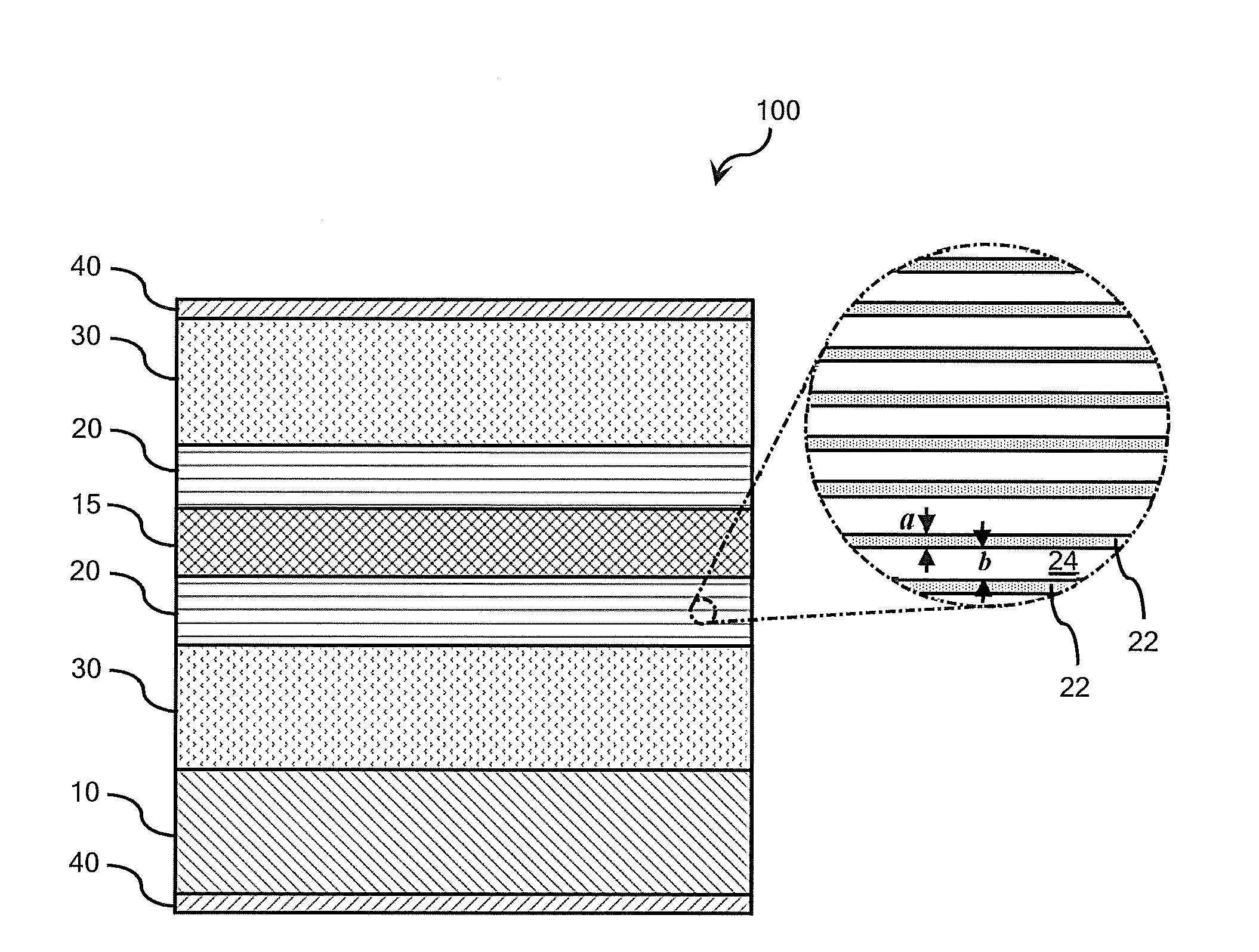
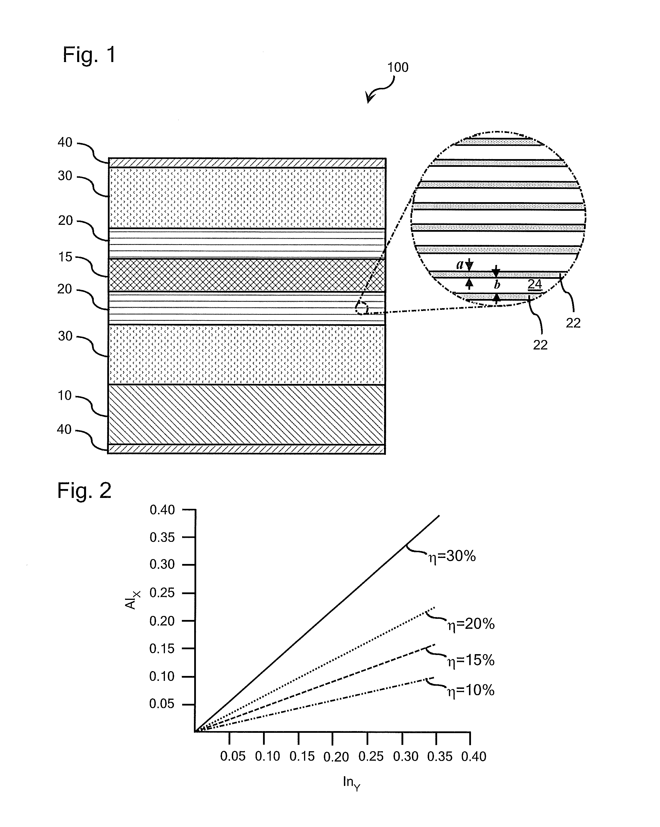
[0030]A laser diode structure comprising the following layers (from bottom to top):[0031]n-GaN buffer layer and cladding layer;[0032]8-12 periods of passive multiple quantum wells, where 2-5 nm passive QWs are separated by 10 nm AlInGaN or AlGaN barriers (for AlGaN, the Al concentration should be 5%-15%), the passive quantum wells are configured to have an emission wavelength 10-40 nm shorter than the lasing wavelength;[0033]2 or 3 periods of InGaN active quantum wells configured to provide optical gain in green spectral range (500-540 nm);[0034]AlInGaN electron blocking layer; and[0035]600-1200 nm thick p-side GaN cladding layer.
example 2
[0036]Similar to Example 1, except an AlInGaN cladding layer is used at least in the n-side cladding layer. This AlInGaN layer lattice matched in one in-plane direction (typically toward c-axis) and has sufficiently low strain in another direction to avoid relaxation. The p-side cladding layer may comprise AlInGaN or AlGaN layer. Each cladding layer may also be made of combination of AlGaN, GaN, InGaN or AlInGaN layers. The structure can also comprise, in addition to strain compensated passive QWs, a bulk InGaN layer or InGaN / GaN superlattice in the waveguide core, to further improve optical confinement. The presence of the strain compensated passive QWs enhances optical confinement, such that high In concentration or large thickness of this bulk layers or superlattices is no longer needed and they can be thin enough to avoid relaxation. Also, due to high refractive index of the passive quantum wells, it is preferred in some designs to position the passive quantum wells between the ...
example 3
[0037]A laser diode structure comprising two passive wells with 5 nm n-AlInGaN barrier below them and 17 nm n-AlInGaN barrier above them. The two passive QWs are separated by 17 nm thick AlInGaN barrier layer. Such structure is placed between the hole blocking layer and the n-InGaN / GaN superlattice with average In concentration 3%-6%. The thickness of the n-superlattice is 114 nm, and it is below the relaxation limit for (20-21) substrate orientation. The n-AlInGaN cladding layer, or the combination of AlInGaN / GaN layers, is placed below the n-InGaN / GaN superlattice layer. The structure also comprises p-InGaN / GaN superlattice with thickness 90 nm. A p-type GaN, AlGaN, AlInGaN, or combination cladding layer may be grown similarly to examples 1 and 2. The structure should also comprise an electron blocking layer between the active region and the cladding layer.
PUM
 Abstract
Description
Claims
Application Information
 - R&D
- Intellectual Property
- Life Sciences
- Materials
- Tech Scout
- Unparalleled Data Quality
- Higher Quality Content
- 60% Fewer Hallucinations
Browse by: Latest US Patents, China's latest patents, Technical Efficacy Thesaurus, Application Domain, Technology Topic, Popular Technical Reports.
© 2025 PatSnap. All rights reserved.Legal|Privacy policy|Modern Slavery Act Transparency Statement|Sitemap|About US| Contact US: help@patsnap.com


