Flat display panel, UV sensor and fabrication method thereof

a technology of ultraviolet light and display panel, which is applied in the field of ultraviolet light (UV) sensors, can solve the problems of increasing uv radiation near the surface of the earth every year, pathological changes in human skin, and difficult for uv-c radiation to reach the earth's surface, and achieves low fabrication cost, high integration probability, and high stability

Active Publication Date: 2013-01-01
AU OPTRONICS CORP
View PDF21 Cites 2 Cited by
  • Summary
  • Abstract
  • Description
  • Claims
  • Application Information

AI Technical Summary

Benefits of technology

[0008]It is one of the primary objectives of the present invention to provide a UV sensor and a flat display panel including a silicon-rich dielectric layer with a refractive index ranging from about 1.7 to about 2.5, so as to solve the above-mentioned problem that conventional UV sensors have low sensitivities or have difficulties in integrating with the fabrication process of semiconductors.
[0013]The UV sensor of the present invention utilizes the silicon-rich dielectric material as the light sensing material to achieve advantages such as high stability, low fabrication cost, and high integrating probability which makes the UV sensor of the present invention suitable in applications with thin film transistors or semiconductor devices, such as flat display panel, so as to raise the added values of the products effectively.

Problems solved by technology

In another aspect, the ozone layer in the atmosphere has long been damaged by chloroflurocarbons (CFCs) emitted by human related activities or other factors, causing the UV radiation near the surface of the earth to increase every year.
Meanwhile, long term exposure under the UV light rays may cause pathological changes to human skins.
Fortunately, it is difficult for UV-C radiation to reach the Earth's surface.
Conventional UV sensors often use group III-V metals such as gallium nitride (GaN) or aluminum gallium nitride (AlGaN) as light sensing materials; however, these materials are often expensive such that the fabrication cost of the UV sensors cannot be effectively reduced.
Also, the UV sensors with GaN or AlGaN materials as light sensing materials possess the issues of heavy contaminations as well as having difficulties to be integrated with semiconductor fabrication process.
Moreover, the UV sensors with GaN or AlGaN materials also possess issues such as over heating of parts during sensing operation, which reduces the sensing performance, making these sensors impractical.
In addition, amorphous silicon thin films or polycrystalline silicon thin films has been conventionally used as the light sensing materials of visible light sensor when integrating photosensor with a display panel; however, the amorphous silicon or the polycrystalline silicon materials are more sensitive to visible light and infrared light rays than UV light rays, and the amorphous silicon and polycrystalline silicon have poor photoelectric conversions as well as poor reliability.
Therefore the amorphous silicon and the polycrystalline silicon materials cannot be applied in UV sensor products effectively.

Method used


Image

  • Flat display panel, UV sensor and fabrication method thereof
  • Flat display panel, UV sensor and fabrication method thereof
  • Flat display panel, UV sensor and fabrication method thereof

Examples


first embodiment

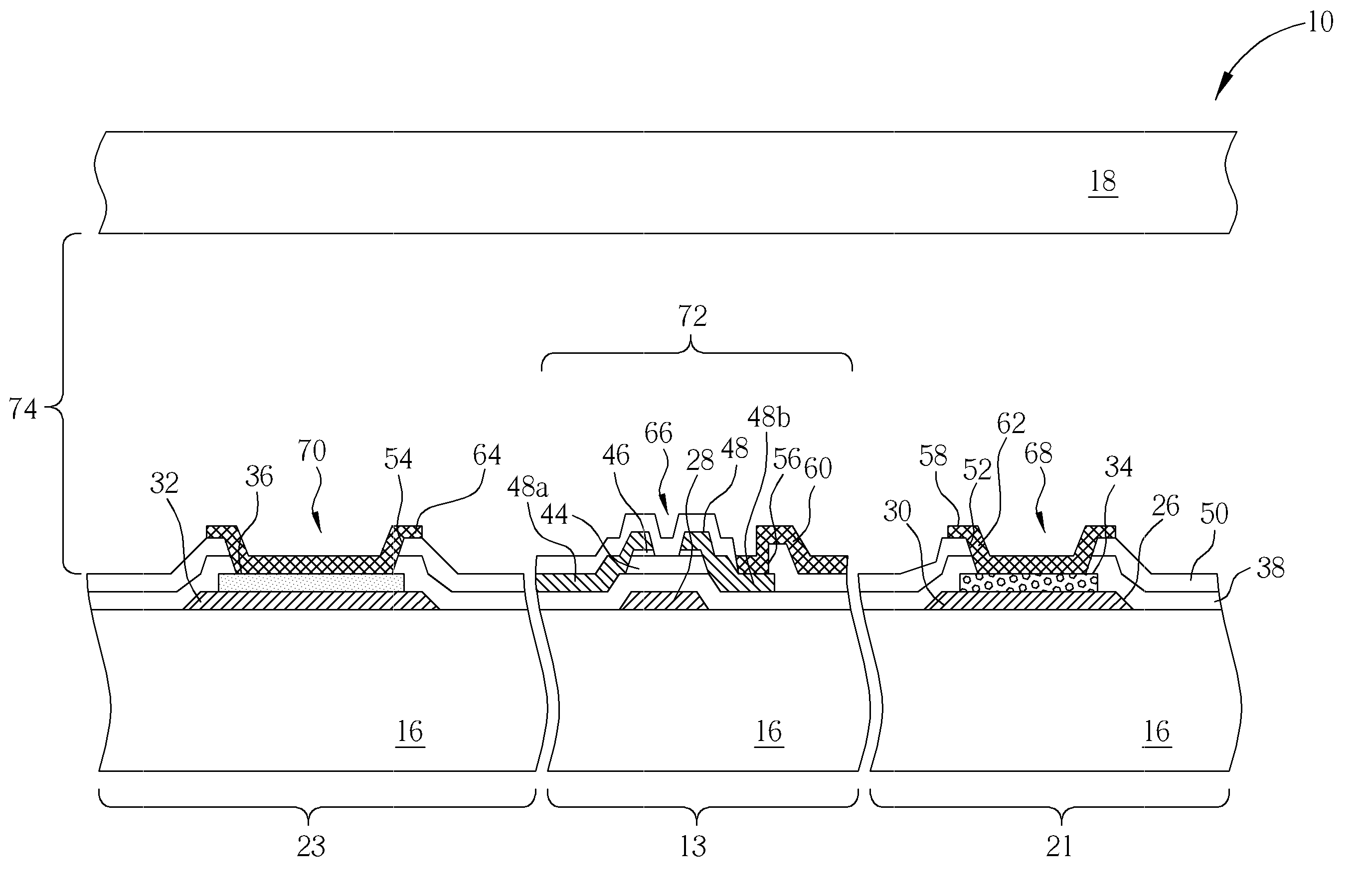
[0024]FIG. 2 to FIG. 4 are partial cross-sectional diagrams illustrating the fabrication method of the flat display panel of the present invention. Referring to FIG. 2, during the fabrication method of the flat display panel 10 of the present invention, a lower substrate 16 is first provided. Then a patterned first conductive layer 26 is formed on the surface of the lower substrate 16. The patterned first conductive layer 26 includes a gate electrode 28, a bottom UV sensing electrode 30, and a bottom visible light sensing electrode 32. The fabrication method of the patterned first conductive layer 26 may include first depositing a first conductive layer (not illustrated) on the surface of the lower substrate 16 and performing a patterning process to the first conductive layer such as a photolithography-etching-process for removing parts of the first conductive layer. After the patterning process, the remaining patterned conductive layer 26 includes the gate electrode 28, the bottom ...

third embodiment

[0034]Referring to FIG. 9, FIG. 9 is a schematic cross-sectional diagram of a flat display panel 100 of the present invention. The flat display panel 100 of the present embodiment is a low temperature polycrystalline silicon (LTPS) display panel. The flat display panel 100 includes a lower substrate 102, an upper substrate 104, and a liquid crystal material layer 106 disposed between the lower substrate 102 and the upper substrate 104. The flat display panel 100 further includes a UV sensor 108 and a plurality of pixel structures 110 disposed in a peripheral region and a display region of the flat display panel 100 respectively. The UV sensor 108 includes at least a UV sensing structure 112 which from bottom to top includes a bottom UV sensing electrode 114, a UV sensing device 116, and a top UV sensing electrode 118. The UV sensing device 116 is composed of a patterned first silicon-rich dielectric layer 120 with a refractive index in a range of about 1.7 to about to about 2.5. Pre...


PUM


Abstract

A UV sensor comprises a silicon-rich dielectric layer with a refractive index in a range of about 1.7 to about 2.5 for serving as the light sensing material of the UV sensor. The fabrication method of the UV sensor can be integrated with the fabrication process of semiconductor devices or flat display panels.

Description

BACKGROUND OF THE INVENTION[0001]1. Field of the Invention[0002]The present invention relates to an ultraviolet (UV) sensor and a fabrication method thereof, and more particularly to a UV sensor including at least a silicon-rich (Si-rich) dielectric material and a fabrication method thereof.[0003]2. Description of the Prior Art[0004]The UV sensors (UVS) have been widely applied in fire hazard monitoring, contamination analyses, astronomical observations, medical facilities, and even military applications. Nowadays, UV sensors are further applied with light emitting diodes with material of Indium Gallium Nitride (InGaN) for example or laser device to form an ultraviolet-blue ray data access system.[0005]In another aspect, the ozone layer in the atmosphere has long been damaged by chloroflurocarbons (CFCs) emitted by human related activities or other factors, causing the UV radiation near the surface of the earth to increase every year. Meanwhile, long term exposure under the UV light...

Claims


Application Information

Patent Timeline
Patent Type & Authority Patents(United States)
IPC IPC(8): H01L21/00
CPCG02F1/13318H01L31/101G02F1/13454G02F2001/133388H01L27/3227G02F1/133388H10K59/60
Inventor CHO, AN-THUNGSHENG, CHI-HUALUO, RUEI-LIANGLIU, WAN-YISUN, WEI-MINHUNG, CHI-MAOCHEN, CHUN-HSIUNHUANG, WEI-MING
Owner AU OPTRONICS CORP
Why Eureka
Try Eureka