Voltage level shifter

a voltage level shifter and shifter technology, applied in the direction of pulse generators, pulse automatic control, electrical apparatus, etc., can solve the problem of indefinite voltage at the output of the pass transistor, and achieve the effect of reducing process cost, reducing leakage, and improving performance characteristics

Inactive Publication Date: 2012-10-09
ARM LTD
View PDF10 Cites 3 Cited by
  • Summary
  • Abstract
  • Description
  • Claims
  • Application Information

AI Technical Summary

Benefits of technology

[0022]The present invention recognises that a voltage level shifter with improved performance characteristics relative to previously known Standard Cell voltage level shifters can be provided by ensuring that the switching circuitry of the voltage level shifter is configured to isolate an output of the pass transistor from the supply voltage rail when the input voltage domain corresponds to a logical zero. This ensures that there is a strong zero at the output of the pass transistor, which in turn ensures correct operation of the pass transistor and avoids the high-threshold phenomenon and the metastability of transistors of the switching circuitry exhibited in previously known voltage level shifter configurations. Isolating the output of the pass transistor from the supply voltage level via the configuration of the switching circuitry results in better slew at the output of the voltage level shifter and allows for a sharper transition between voltage levels.
[0035]In one embodiment, the voltage level shifter comprises a single voltage domain NWELL. This enables the area of the voltage level shifter to be reduced relative to the dual NWELL design and reduces the process cost by offering a lower resolution NWELL mask for fabrication.

Problems solved by technology

In previously known voltage level shifters having single NWELL designs (i.e. ones that are not suitable for implementation in Standard Cell libraries) the switching circuitry provides only half feedback and this can give rise to an indefinite voltage at the output of the pass transistor.

Method used


Image

  • Voltage level shifter
  • Voltage level shifter
  • Voltage level shifter

Examples


first embodiment

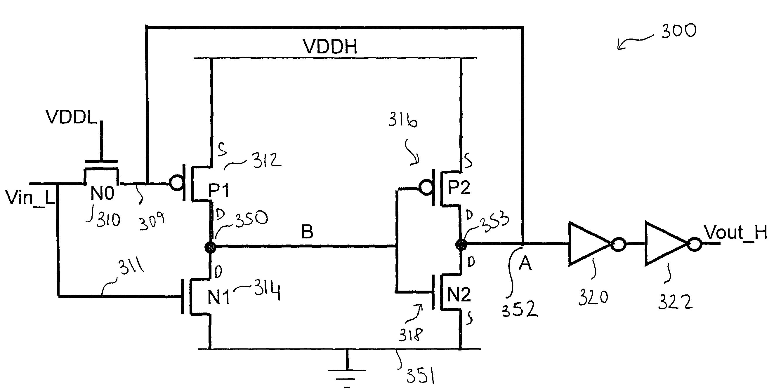
[0054]FIG. 3 schematically illustrates a Single-well voltage level shifter design suitable for a Standard Cell according to the present invention. The circuit comprises an NMOS pass transistor 310 and four transistors 312, 314, 316, 318 connected between a high voltage domain VDDH (source voltage) and a ground voltage rail 351. These four transistors comprise a first PMOS transistor 312 whose gate is connected to the output of the pass transistor 310 and whose source is connected to the high voltage domain VDDH. The drain of the PMOS transistor 312 is connected to the drain of an NMOS transistor 314 and the source of that NMOS transistor 314 is in turn connected to the ground rail 351.

[0055]The pair of transistors comprising the PMOS transistor 316 and the NMOS transistor 318 together form an inverter circuit. The source of the PMOS transistor 316 is connected to the high voltage domain VDDH, whereas the source of the NMOS transistor 318 is connected to the ground voltage rail 351. ...

second embodiment

[0066]FIG. 6 schematically illustrates a single well voltage level system according to the present invention. The circuit of FIG. 6 is functionally equivalent to the circuit of FIG. 3, but instead of CMOS transistors, the circuit is constructed using Carbon Nano Tube Field Effect Transistors (CNTFETs). The circuit of FIG. 6 is structurally similar to the arrangement of FIG. 3, with the exception that the inverters 320, 322 (on output path) in FIG. 3 are each replaced by a pair of CNTFET transistors and are both connected to both the high voltage domain VDDH and the ground voltage VFS.

[0067]The circuit 600 of FIG. 6 comprises a pass transistor 610, a set of four switching CNTFET transistor 612, 614, 616, 618 corresponding respectively to the transistors 312, 314, 316 and 318 of FIG. 3. The transistors 612, 616 whose sources are connected to VDDH each have a diameter d1 whereas the transistors 614, 618 each have a diameter of d2. Similarly to the arrangement of FIG. 3 the transistors ...


PUM


Abstract

A voltage level shifter is provided for receiving an input signal from an input voltage domain and converting said signal to a shifted signal in a shifted voltage domain. The voltage level shifter has an input, switching circuitry, a pass transistor and an output. The switching circuitry is configured to isolate an output of said pass transistor from said supply voltage rail when said input voltage domain corresponds to a logical zero.

Description

[0001]This application claims priority to U.S. Provisional Application No. 61 / 222,673, filed Jul. 2, 2009, the entire contents of which are hereby incorporated by reference.BACKGROUND OF THE INVENTION[0002]1. Field of the Invention[0003]The field of the invention relates to voltage level shifters for shifting the voltage level between two different voltage domains.[0004]2. Description of the Prior Art[0005]It is known to provide voltage level shifters to convert a signal from one voltage domain to a signal suitable for another voltage domain. This allows circuits that operate different voltage levels to interface with each other.[0006]In the design of Application Specific Integrated Circuits (ASIC), circuit design is often performed via the implementation of Standard Cells. In this way ASIC manufacturers can create functional blocks with known electrical characteristics such as propagation delay, capacitance and inductance that can be represented in third party circuit design tools....

Claims


Application Information

Patent Timeline
Patent Type & Authority Patents(United States)
IPC IPC(8): H03L5/00
CPCH03K19/018521H03K3/356113
Inventor ALAM, AKHTAR W
Owner ARM LTD
Why Eureka
Try Eureka