Method for fabricating circuit board structure with capacitors embedded therein

a technology of capacitors and circuit boards, applied in the direction of printed capacitor incorporation, printed element electric connection formation, conductive pattern formation, etc., can solve the problems of reduced flexibility of wiring layout on the surface, unfavorable shrinkage of package size, and increased noise, so as to achieve the effect of more capacitan

Active Publication Date: 2012-09-04
UNIMICRON TECH CORP
View PDF4 Cites 0 Cited by
  • Summary
  • Abstract
  • Description
  • Claims
  • Application Information

AI Technical Summary

Benefits of technology

[0010]In view of the above prior art disadvantages, the object of the present invention is to provide a circuit board structure with capacitors embedded therein and fabricating method thereof, whereby advanced flexibility of layouts of both the electrode plates and the circuits on the circuit board and parallel connection between the capacitors to provide more capacitance are achieved.
[0021]Accordingly, the present invention can improve the flexibility of circuit layout, realize parallel connection between the capacitors to provide more capacitance, efficiently enhance the utilization ratio of inner space of the circuit board, and thereby achieve the purpose of miniaturization.

Problems solved by technology

However, as the density of wiring in a package structure increases, the noise also increases.
In conventional methods, utilizing surface mount technology (SMT) integrates most passive components onto a surface of a packaging substrate, such that the flexibility of wiring layout on the surface is restricted, and the occupied space is unfavorable to shrinkage of package size.
However, the prior art forms a whole piece of high dielectric constant material layer within a packaging substrate, wherein the used part of the high dielectric constant material layer for a capacitor is merely the one between the inner electrode plate and the outer electrode plate, while the unused part of the high dielectric constant material layer electrically contacts with the circuits, such that the structure has several drawbacks: first, the unused part of the high dielectric constant material layer causes waste, unfavorable to reducing the cost; second, owing to the poor fluidity of the high dielectric constant material, voids and poor uniformity of thickness occur; third, the unused part of the high dielectric constant material layer contacts the circuits, so that parasitic capacitance occurs to interfere with electrical qualities; finally, because the electrode plates and the circuits are laid together in a circuit layer, the flexibility of layouts of both the electrode plates and the circuits is compromised.
However, in the structure, the electrode plates and the circuits are still laid together in a circuit layer, such that the flexibility of layouts of both the electrode plates and the circuits is compromised, and parallel connection between the capacitors to provide more capacitance cannot be achieved.

Method used


Image

  • Method for fabricating circuit board structure with capacitors embedded therein
  • Method for fabricating circuit board structure with capacitors embedded therein
  • Method for fabricating circuit board structure with capacitors embedded therein

Examples


embodiment 1

Method Embodiment 1

[0028]With reference to FIGS. 3A to 3D, there are shown cross-section views of a process for fabricating a circuit board structure with capacitors embedded therein. As shown in FIG. 3A, at least two core layers 3,3 are provided. In the present embodiment, three core layers 3, 3′, and 3 are provided, and the core layers 3, 3′ and 3 individually comprise a dielectric layer 31. The material of the dielectric layer 31 can be selected from the group consisting of a non-photosensitive organic resin, a photosensitive organic resin (e.g. ABF (Ajinomoto Build-up Film), BCB (Benzocyclo-buthene), LCP (Liquid Crystal Polymer), PI (Poly-imide), PPE (Poly(phenylene ether)), PTFE (Poly(tetra-fluoroethylene)), FR4, FR5, BT (Bismaleimide Triazine), or Aramide), and a mixture of epoxy resin and fiber glass. In the present embodiment, the material of the dielectric layer 31 is ABF. The dielectric layer 31 has two opposite surfaces, and the outsides of the two opposite surfaces indiv...

embodiment 2

Method Embodiment 2

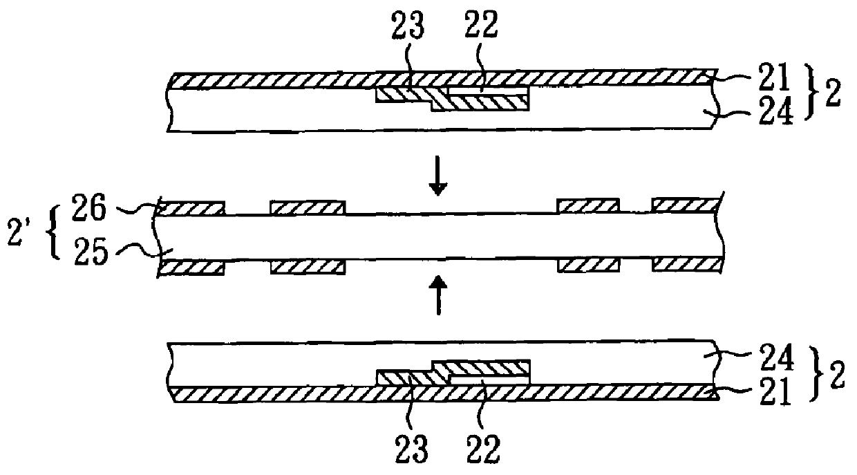
[0034]With reference to FIGS. 4A to 4F, there are shown cross-section views of another process for fabricating a circuit board structure with capacitors embedded therein. As shown in FIG. 4A, a first core layer 5 is provided. The first core layer 5 comprises a dielectric layer 51 having two opposite surfaces, first metal layers 52 disposed on the outsides of the two opposite surfaces of the dielectric layer, and at least two capacitors 53 embedded respectively on the insides of the two opposite surfaces of the dielectric layer 51 and individually electrically connecting with the first metal layer 52 at the same side.

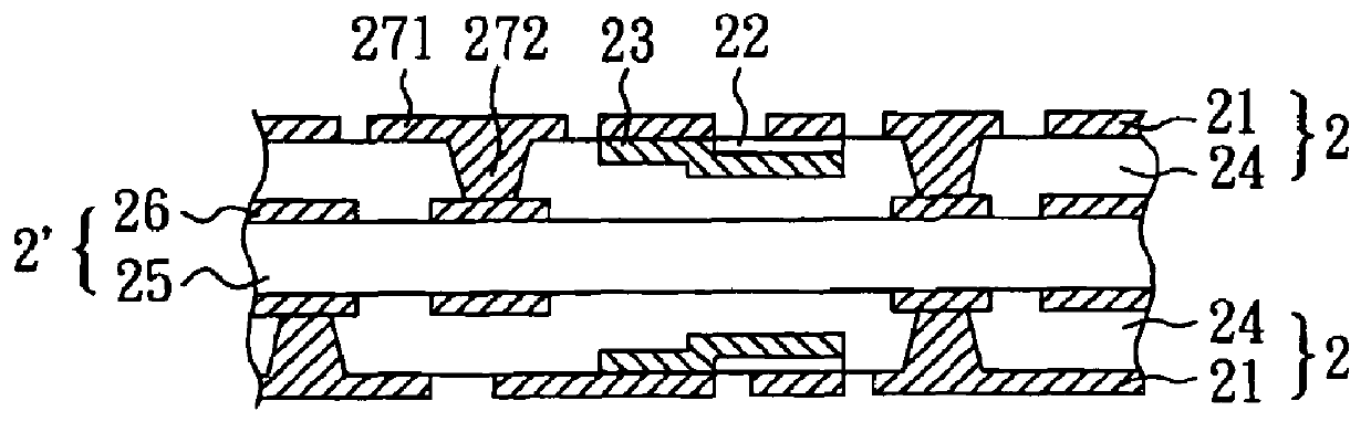
[0035]Subsequently, as shown in FIG. 4B, a second core layer 6 and a third core layer 7 are provided. The second core layer 6 and the third core layer 7 individually comprise a dielectric layer 61,71; a first metal layer 62,72 disposed on one surface of the dielectric layer 61,71; and at least one capacitor 61,71 embedded on the inside of the surface w...

embodiment 3

Method Embodiment 3

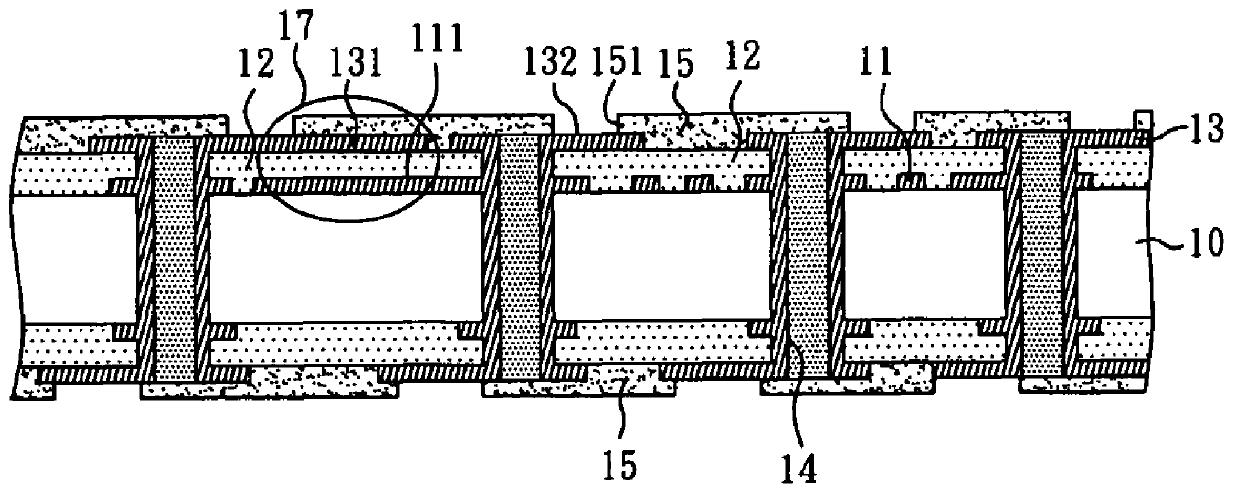
[0041]The present embodiment is the same as Method Embodiment 2, except the process for fabricating the components electrically connecting the circuit layers 521, 621 and 721. Please refer to FIG. 5A. In the present embodiment, a second conductive through hole 54 is formed in the first core layer 5, and the second conductive through hole 54 electrically connects the circuit layers 521 on the two sides of the first core layer 5. After the first core layer 5 is laminated between the second core layer 6 and the third core layer 7, a plurality of vias 610 and 710 are formed in the second core layer 6 and the third core layer 7, respectively. Then, the first metal layers of the second core layer 6 and the third core layer 7 are patterned to form circuit layers 621 and 721, respectively, and conductive vias 622 and 722 are simultaneously formed in the vias 610 and 710, respectively. Other steps are the same as those described in Method Embodiment 2. The conductive vias ...


PUM

PropertyMeasurementUnit
dielectric constantaaaaaaaaaa

Abstract

A circuit board structure with capacitors embedded therein and a method for fabricating the same are disclosed. The structure comprises at least two core layers individually comprising a dielectric layer having two opposite surfaces, circuit layers disposed on the outsides of the two opposite surfaces of the dielectric layer, and at least two capacitors embedded respectively on the insides of the two opposite surfaces of the dielectric layer and individually electrically connecting with the circuit layer at the same side; at least one adhesive layer disposed between the core layers to combine the core layers as a core structure; and at least one conductive through hole penetrating the core layers and the adhesive layer, and electrically connecting the circuit layers of the core layers. Accordingly, the present invention can improve the flexibility of circuit layout, and realize parallel connection between the capacitors to provide more capacitance.

Description

BACKGROUND OF THE INVENTION[0001]1. Field of the Invention[0002]The present invention relates to a circuit board structure with capacitors embedded therein and a method for fabricating the same and, more particularly, to a circuit board structure with capacitors embedded therein and a method for fabricating the same, which can improve the flexibility of circuit layout.[0003]2. Description of Related Art[0004]Currently, the relentless progress in semiconductor fabricating process and electronic functions of microelectronic devices has lead to a highly integrated development of semiconductor chips. Quantity of input / output terminals and density of wiring in package structures increase as semiconductor chips develop toward high integration. However, as the density of wiring in a package structure increases, the noise also increases. Generally, in order to obviate noise or compensate electricity, passive components, e.g. resistors, capacitors, and inductors, are installed in a semicondu...

Claims


Application Information

Patent Timeline
Patent Type & Authority Patents(United States)
IPC IPC(8): H05K1/16H05K3/02H05K3/46H05K3/42H05K3/32
CPCH05K1/162H05K2201/09536H05K3/4652Y10T29/49156Y10T29/49126Y10T29/4913Y10T29/49155H05K2201/09763H05K3/4611H05K3/4602H05K3/429H05K2201/0355Y10T29/49165
Inventor LIEN, CHUNG-CHENGYANG, CHIH-KUI
Owner UNIMICRON TECH CORP
Why Eureka
Try Eureka