Solid-state image sensing device, method for reading signal of solid-state image sensing device, and image pickup apparatus
a solid-state image and sensing device technology, applied in the direction of color television details, television systems, radio control devices, etc., can solve the problems of difficult to reduce the chip size of cmos image sensors, and achieve the effect of reducing the circuit area, reducing the size of the body of the image pickup apparatus, and reducing the chip size of the solid-state image sensing devi
- Summary
- Abstract
- Description
- Claims
- Application Information
AI Technical Summary
Benefits of technology
Problems solved by technology
Method used
Image
Examples
application example 1
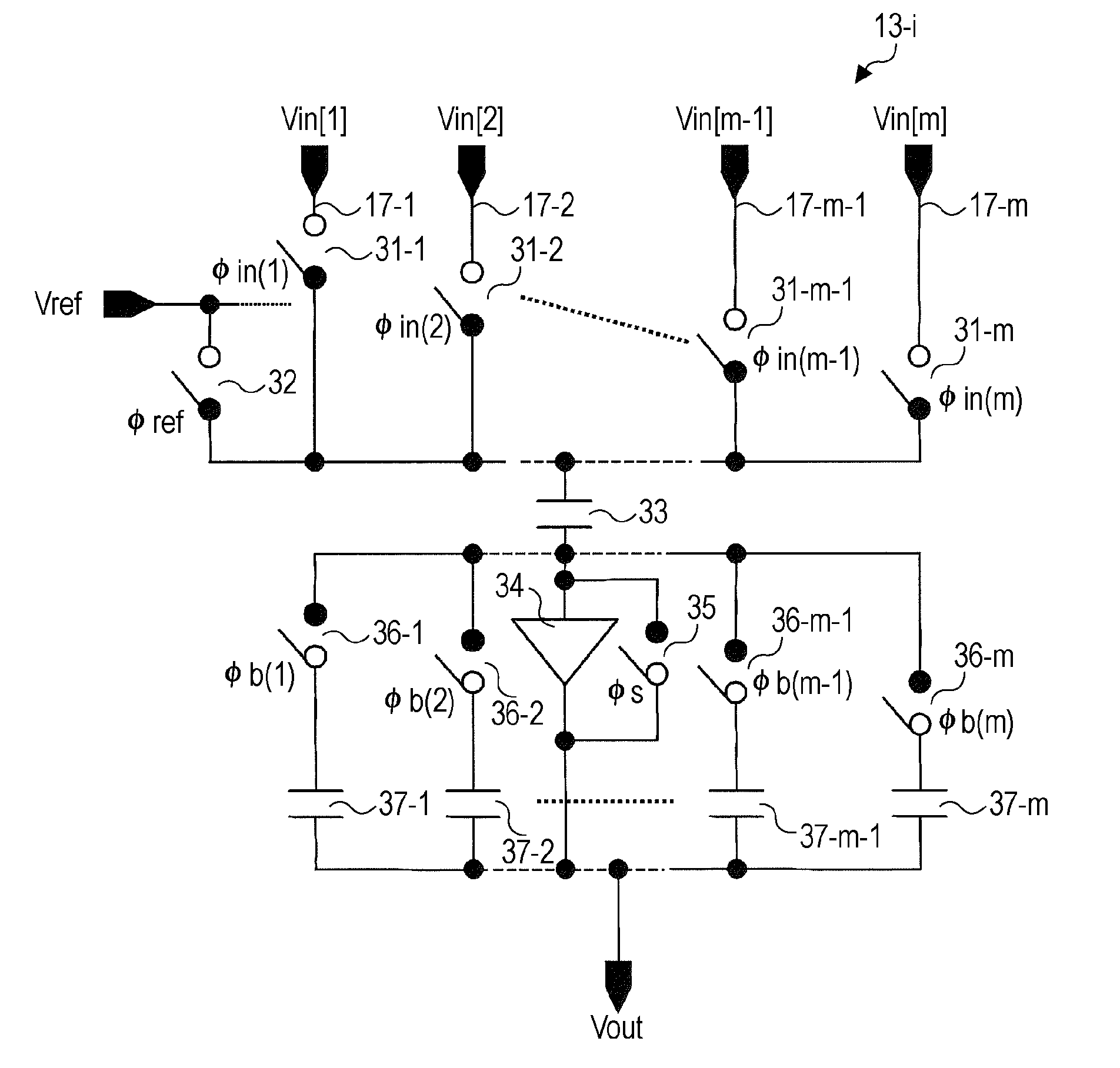
[0111]FIG. 8 is a circuit diagram illustrating a circuit configuration of a unit readout circuit 13-iA according to an application example 1. The same numbering will be used in describing FIG. 8 as was utilized above in describing FIG. 3, where appropriate.
[0112]As shown in FIG. 8, the unit readout circuit 13-iA of the application example 1 uses a variable capacitor for the feedback capacitor 37-i (37-1 to 37-m). Thus, the capacitance value C2(i) of the feedback capacitor 37-i is variable. The signal level of the received-light photoelectric conversion signal Vsig from the unit pixel 20 is monitored by, for example, the system control unit 15 for each of the columns of the pixel array. Thereafter, the system control unit 15 performs control so that, when the signal levels of the received-light photoelectric conversion signal Vsig output from all of the columns or more than a predetermined number of columns are less than a predetermined value, the capacitance value C2(i) of the feedb...
application example 2
[0114]FIG. 9 is a circuit diagram illustrating a circuit configuration of a unit readout circuit 13-iB according to an application example 2. The same numbering will be used in describing FIG. 9 as was utilized above in describing FIG. 8, where appropriate.
[0115]As shown in FIG. 9, like the unit readout circuit 13-iA according to the application example 1, the unit readout circuit 13-iB of the application example 2 uses a variable capacitor for the feedback capacitor 37-i (37-1 to 37-m). In addition, the unit readout circuit 13-iB includes a comparator 38 for comparing the signal level of the received-light photoelectric conversion signal Vsig from the unit pixel 20 in each of the columns of the pixel array with a predetermined value and a controller 39 for controlling the capacitance value C2(i) of the feedback capacitor 37-i on the basis of the comparison result output from the comparator 38. In this way, the capacitance value C2(i) of the feedback capacitor 37-i is adaptively cha...
application example 3
[0128]A unit readout circuit of an application example 3 has a circuit configuration similar to that shown in FIG. 3. However, by using different control timing points, the unit readout circuit can have a signal integration function that takes the integral of the signal values.
[0129]More specifically, by switching between the reset signal Vreset and the reference voltage Vref for the same column of the pixel array M times (M is an integer greater than or equal to 2) instead of once, a signal M-(Vreset(i)−Vref) obtained by multiplying the reset signal Vreset by M can be acquired. Thereafter, similarly, by switching between the reference voltage Vref and the received-light photoelectric conversion signal M times, the following output signal Vout(i) can be eventually obtained:
Vout(i)=M·C1 / C2(i)·(Vreset(i)−Vsig(i)).
[0130]FIG. 11 illustrates control timing used when M integration operations are performed for each of the columns. When the operation is performed for m columns, the computat...
PUM
 Abstract
Description
Claims
Application Information
 - R&D
- Intellectual Property
- Life Sciences
- Materials
- Tech Scout
- Unparalleled Data Quality
- Higher Quality Content
- 60% Fewer Hallucinations
Browse by: Latest US Patents, China's latest patents, Technical Efficacy Thesaurus, Application Domain, Technology Topic, Popular Technical Reports.
© 2025 PatSnap. All rights reserved.Legal|Privacy policy|Modern Slavery Act Transparency Statement|Sitemap|About US| Contact US: help@patsnap.com


