Surface emitting laser with trenches to define conductive regions

a surface emitting laser and trench technology, applied in semiconductor lasers, instruments, recording devices, etc., can solve the problems of reducing the reliability of the resulting device and the yield, and achieve the effect of ensuring the reliability of the device and small preparation error

Inactive Publication Date: 2012-05-29
CANON KK
View PDF14 Cites 1 Cited by
  • Summary
  • Abstract
  • Description
  • Claims
  • Application Information

AI Technical Summary

Benefits of technology

[0016]The present invention provides a surface emitting laser including a plurality of current confinement structures in which a preparation error is small and the reliability of a device can be ensured, and a method for producing the same.
[0018]According to the present invention, it is possible to provide a surface emitting laser including a plurality of current confinement structures in which a preparation error is small and the reliability of a device can be ensured, and a method for producing the same.

Problems solved by technology

However, according to empirical facts, with an increase in the oxidation distance, it becomes difficult to control the oxidation process and the probability in which the oxidation distance does not match with a design value increases, resulting in a decrease in the yield.
In addition, when the oxidation distance increases, the resulting oxidized layer tends to be detached from adjacent semiconductor layers during an annealing treatment or during current injection, resulting in a decrease in the reliability of the resulting device.

Method used


Image

  • Surface emitting laser with trenches to define conductive regions
  • Surface emitting laser with trenches to define conductive regions
  • Surface emitting laser with trenches to define conductive regions

Examples


first embodiment

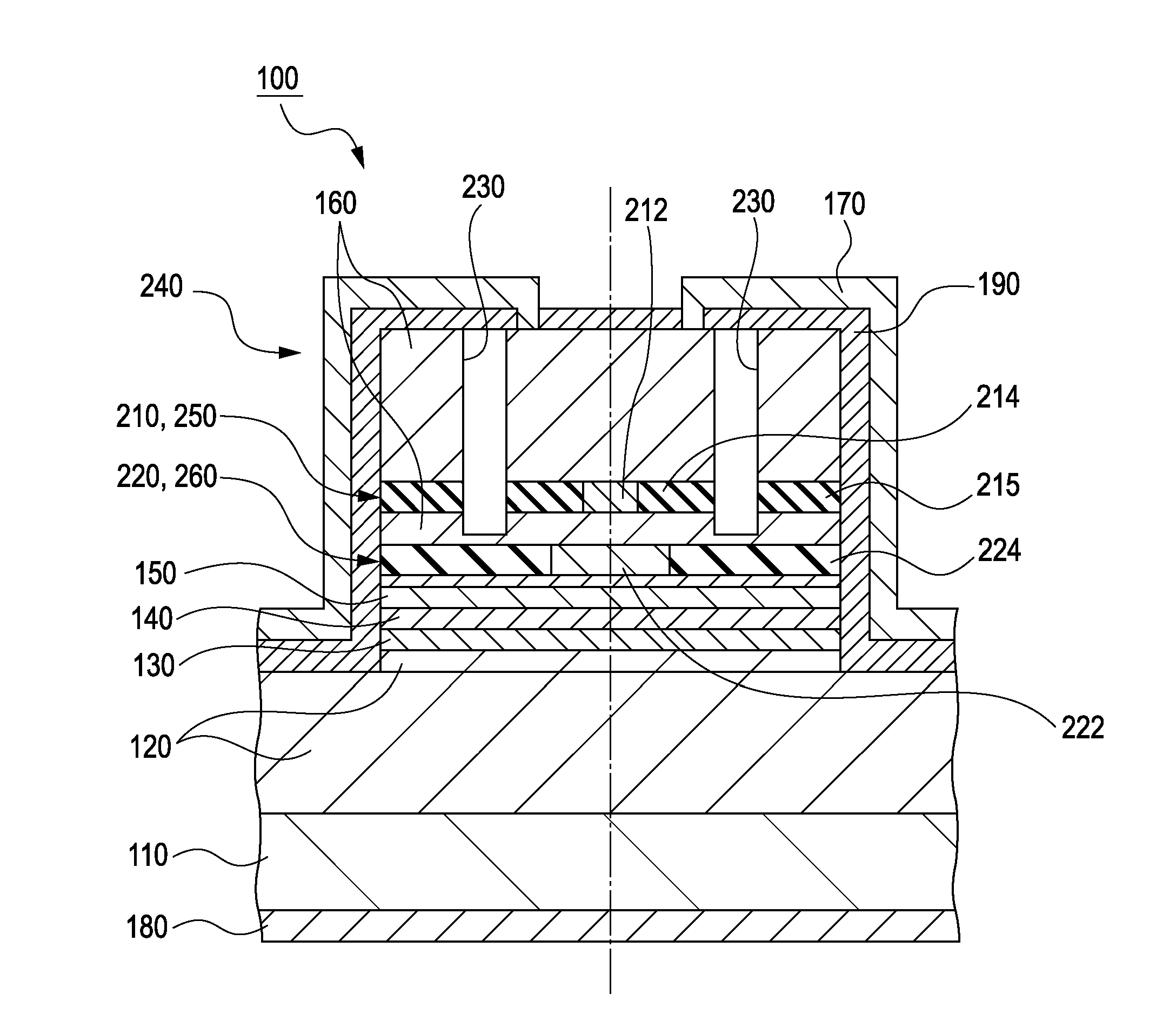
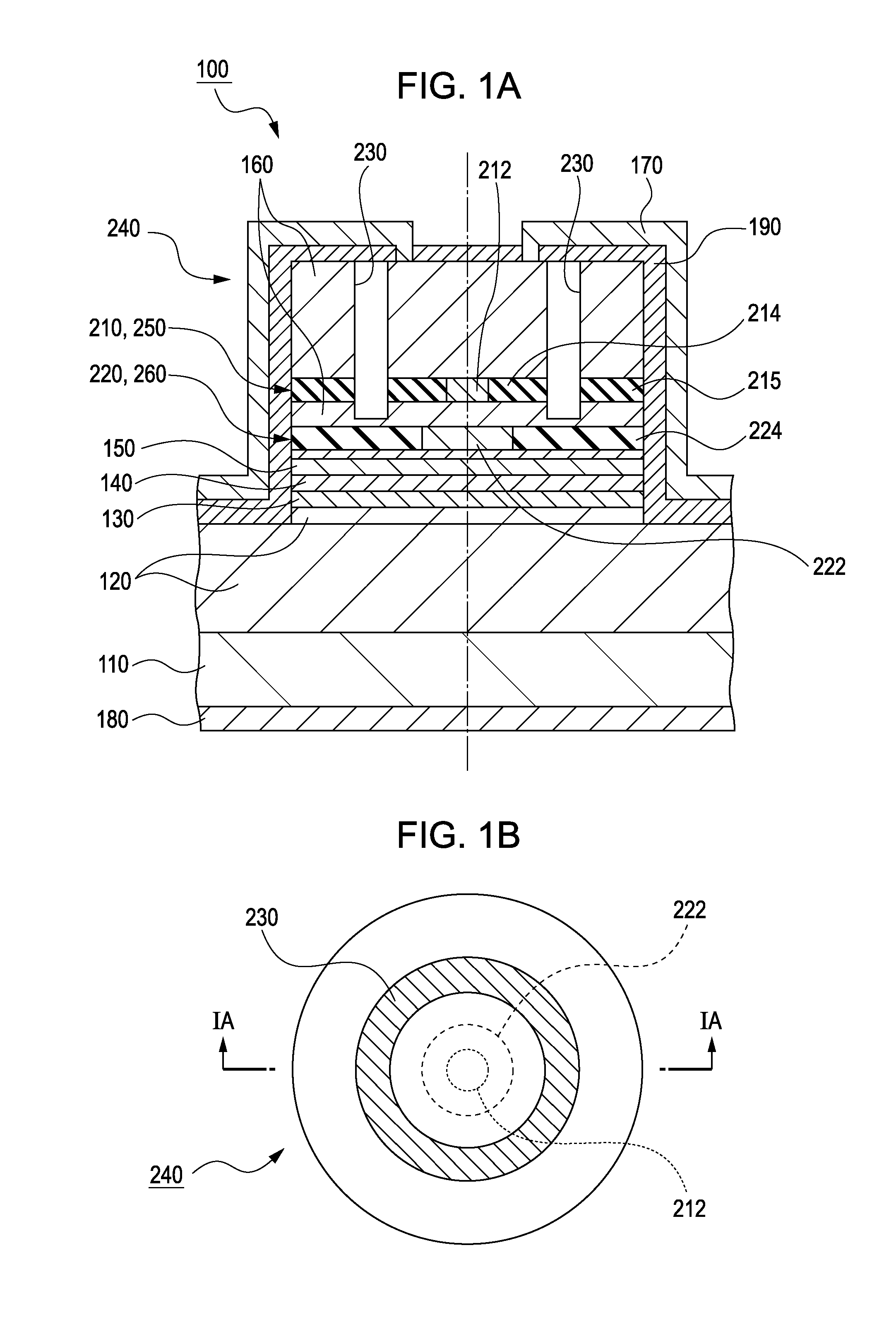
[0032]FIG. 1A is a schematic cross-sectional view of a surface emitting laser 100 according to a first embodiment of the present invention, and FIG. 1B is a schematic top view of the surface emitting laser 100. Specifically, FIG. 1A is a cross-sectional view taken along line IA-IA in FIG. 1B.

[0033]A lower multilayer mirror 120, a lower spacer layer 130, an active layer 140, an upper spacer layer 150, and an upper multilayer mirror 160 are stacked on a substrate 110 in that order to form a laser cavity in a direction perpendicular to a substrate surface. Carriers (electrons or holes-depending on the type of doping) are injected from an upper electrode 170 provided on the upper multilayer mirror 160 and a lower electrode 180 provided below the substrate 110 into the active layer 140. The active layer 140 emits light, thus leading to the oscillation of the surface emitting laser 100.

[0034]A first current confinement layer 210 is provided in the upper multilayer mirror 160. The first cu...

second embodiment

[0128]FIG. 7A is a schematic cross-sectional view of a surface emitting laser according to a second embodiment of the present invention, and FIG. 7B is a schematic top view of the surface emitting laser according to the second embodiment of the present invention. Specifically, FIG. 7A is a cross-sectional view taken along line VIIA-VIIA in FIG. 7B. Components that are common to those in the first embodiment are assigned the same reference numerals shown in FIGS. 1A to 6; thus, repetitive description thereof may be omitted.

[0129]A feature of the second embodiment is that a first trench structure 230 is divided into a plurality of portions. Therefore, carriers can flow into a first electrically conductive region 212 also from a region located above a first current confinement layer 210 and outside the first trench structure 230 when viewed from the central portion of an upper multilayer mirror 160 of the device. Accordingly, as shown in FIG. 7B, a contact region 175 can be formed even...

third embodiment

[0138]FIG. 8A is a schematic cross-sectional view of a surface emitting laser according to a third embodiment of the present invention. FIG. 8B is a schematic top view of the surface emitting laser according to the third embodiment of the present invention. Specifically, FIG. 8A is a cross-sectional view taken along line VIIIA-VIIIA in FIG. 8B.

[0139]As shown in FIGS. 8A and 8B, a third trench structure 280 can be provided on an emission aperture of the surface emitting laser of the first embodiment or the second embodiment. In FIG. 8B, a first electrically conductive region 212 is omitted for simplicity.

[0140]The third trench structure 280 has a function of providing an in-plane distribution of the reflectivity of an upper multilayer mirror 160, viewed from the active layer side, in a light-emitting region (specifically, in a second electrically conductive region 222). For this purpose, the third trench structure 280 is arranged inside the second electrically conductive region 222 i...


PUM


Abstract

A surface emitting laser includes a lower multilayer mirror, an active layer, and an upper multilayer mirror stacked onto a substrate. A first current confinement layer having a first electrically conductive region and a first insulating region is formed above or below the active layer using a first trench structure. A second current confinement layer having a second electrically conductive region and a second insulating region is formed above or below the first current confinement layer using a second trench structure. The first and second trench structures extend from a top surface of the upper multilayer mirror towards the substrate such that the second trench structure surrounds the first trench structure. When the surface emitting laser is viewed in an in-plane direction of the substrate, a boundary between the first electrically conductive region and the first insulating region is disposed inside the second electrically conductive region.

Description

BACKGROUND OF THE INVENTION[0001]1. Field of the Invention[0002]The present invention relates to a surface emitting laser, a method for producing a surface emitting laser, and an image forming apparatus.[0003]2. Description of the Related Art[0004]A vertical cavity surface emitting laser (VCSEL) is a surface emitting laser capable of emitting light in a direction perpendicular to a substrate surface and has a feature that a two-dimensional array can be easily formed.[0005]Densification and high-speed operation can be realized by the parallel processing of a plurality of beams emitted from the two-dimensional array, and various industrial applications such as optical communication are expected. For example, when a surface emitting laser array is used as a light source for exposure of an electrophotographic printer, densification and high-speed operation can be achieved in a step of forming an image using a plurality of beams.[0006]In such electrophotographic application, it is necess...

Claims


Application Information

Patent Timeline
Patent Type & Authority Patents(United States)
IPC IPC(8): H01L29/26
CPCH01S5/18311H01S5/0286H01S5/18313H01S5/18316H01S5/18333H01S5/18347Y10S257/918
Inventor IKUTA, MITSUHIRO
Owner CANON KK
Why Eureka
Try Eureka