Non-volatile memory including assist gate

a non-volatile memory and assist gate technology, applied in the field of semiconductor devices, can solve the problems of increasing programming disturbance and serious electrical interference of memory cells

Active Publication Date: 2009-05-05
POWERCHIP SEMICON MFG CORP
View PDF2 Cites 0 Cited by
  • Summary
  • Abstract
  • Description
  • Claims
  • Application Information

AI Technical Summary

Benefits of technology

[0011]Accordingly, at least one objective of the present invention is to provide a non-volatile memory and manufacturing method thereof capable of providing a definite gate-coupling ratio and device reliability for the memory cells therein.
[0012]At least a second objective of the present invention is to provide a non-volatile memory and manufacturing method thereof capable of reducing the dimension of the memory cells therein and increasing the level of device integration.
[0013]At least a third objective of the present invention is to provide a non-volatile memory and manufacturing method thereof having a simpler fabrication process so that the production cost is reduced.

Problems solved by technology

As a result, assist gate leakage between neighboring memory cells will easily occur when the memory cells are programmed and hence lead to an increase in programming disturbance.
Thus, the electrical performance of the memory cells can be seriously affected.

Method used


Image

  • Non-volatile memory including assist gate
  • Non-volatile memory including assist gate
  • Non-volatile memory including assist gate

Examples


Embodiment Construction

[0035]Reference will now be made in detail to the present preferred embodiments of the invention, examples of which are illustrated in the accompanying drawings. Wherever possible, the same reference numbers are used in the drawings and the description to refer to the same or like parts.

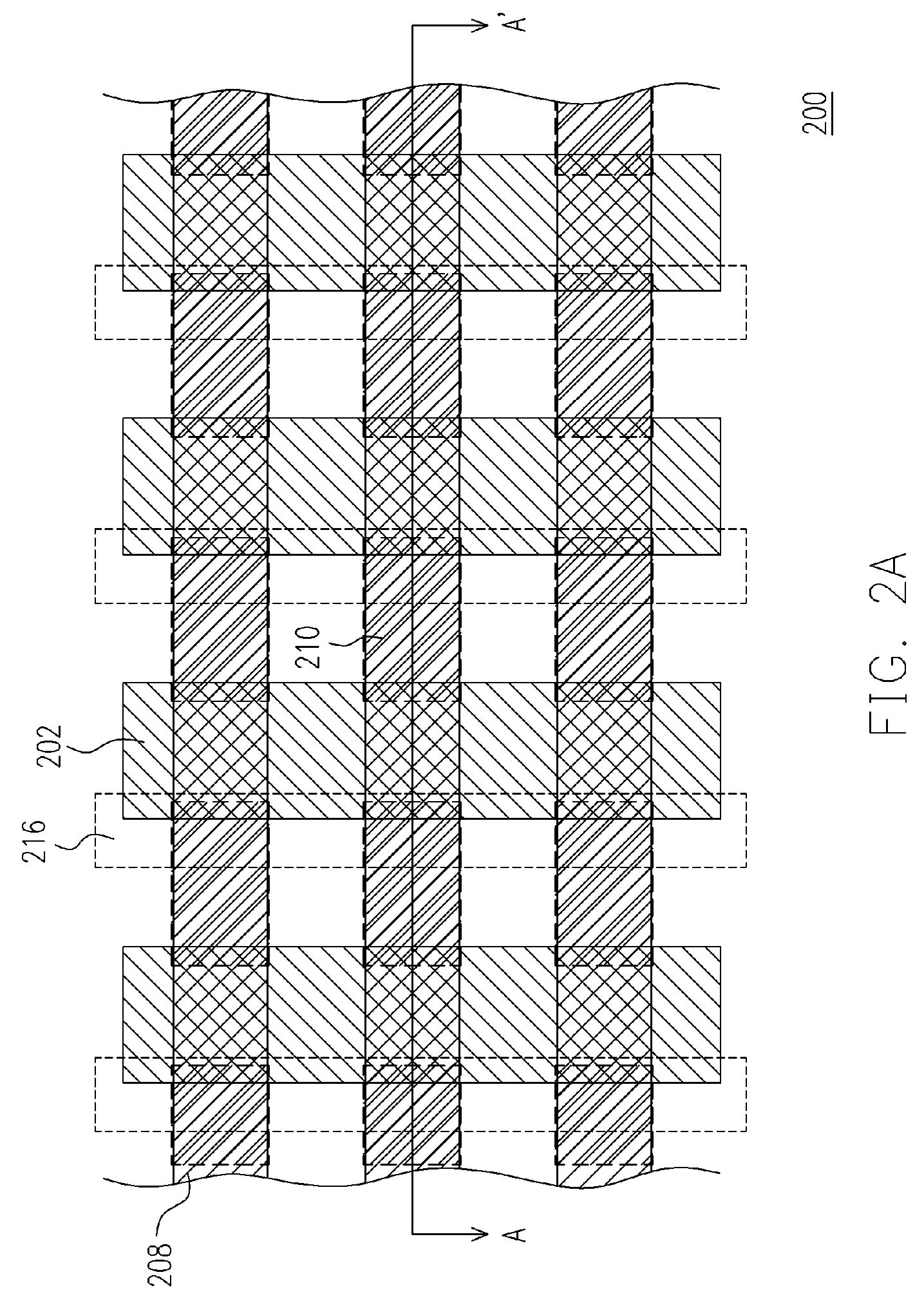
[0036]FIG. 2A is a top view of a non-volatile memory according to the present invention. FIG. 2B is a cross-sectional view along line A-A′ of FIG. 2A. FIG. 2C is a simplified circuit diagram of the non-volatile memory according to the present invention.

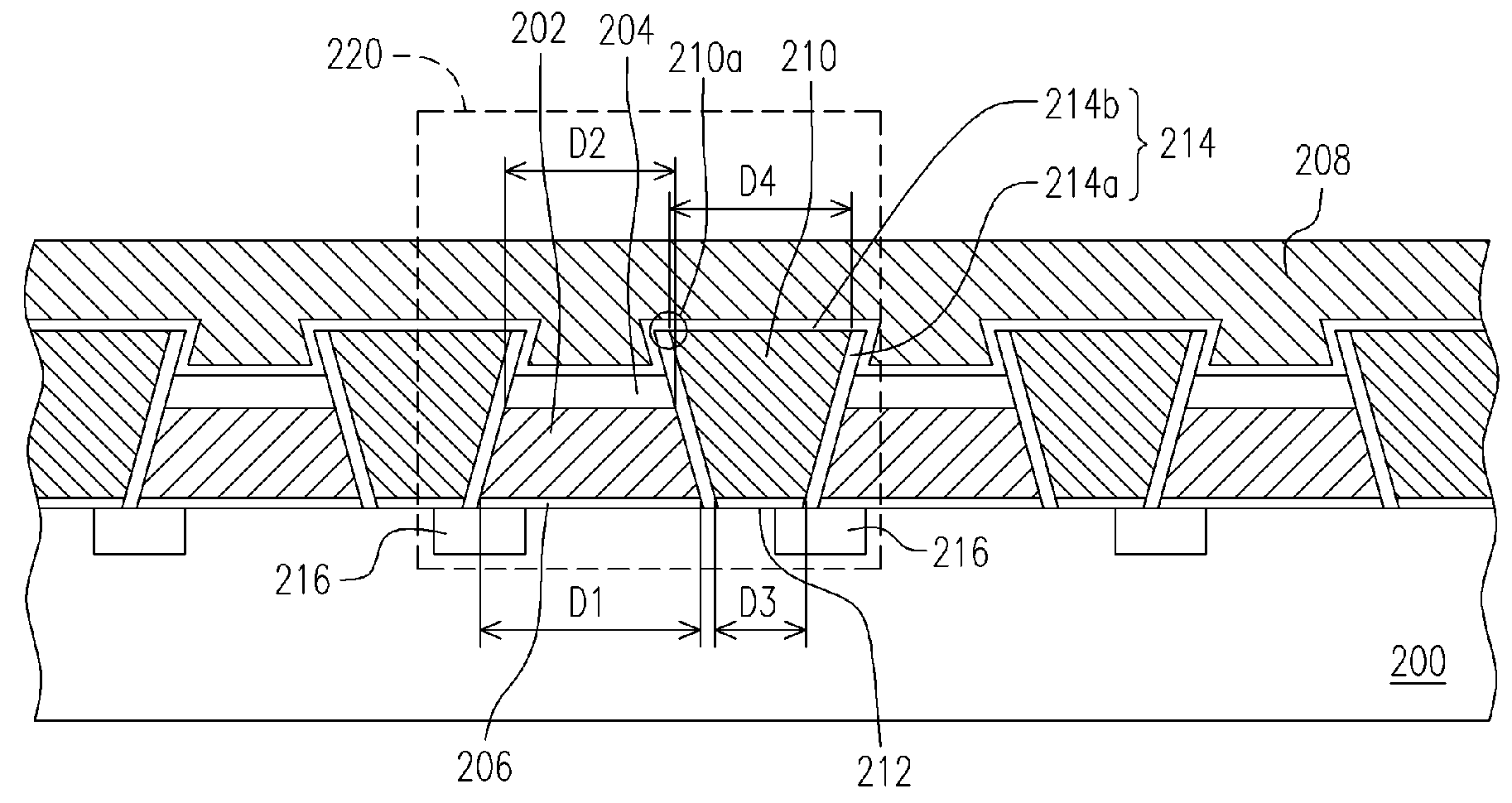
[0037]As shown in FIGS. 2A and 2B, the non-volatile memory of the present invention includes a substrate 200, a plurality of assist gates 202, a plurality of cap layers 204, a plurality of gate dielectric layers 206, a plurality of word lines 208, a plurality of floating gates 210, a plurality of tunneling dielectric layers 212, a plurality of inter-gate dielectric layers 214 (each including an inter-gate dielectric layer 214a and an inter-gate dielect...


PUM


Abstract

A non-volatile memory is provided. An assist gate structure is formed on a substrate such that the width at the bottom of the assist gate structure is greater than the width at the top of the assist gate structure. A floating gate is formed on one side of the assist gate structure and disposed between a word line and the substrate. The width at the bottom of the floating gate is smaller than the width at the top of the floating gate. The word line, the floating gate and the assist gate structure together form a memory unit. A tunneling dielectric layer is formed between the floating gate and the substrate. An inter-gate dielectric layer is formed between the word line, the floating gate and the assist gate structure. Source / drain regions are formed in the substrate on the respective sides of the memory unit.

Description

CROSS-REFERENCE TO RELATED APPLICATION[0001]This application claims the priority benefit of Taiwan application serial No. 94105555, filed on Feb. 24, 2005. All disclosure of the Taiwan application is incorporated herein by reference.BACKGROUND OF THE INVENTION[0002]1. Field of the Invention[0003]The present invention relates to a semiconductor device. More particularly, the present invention relates to a non-volatile memory and a manufacturing method thereof.[0004]2. Description of the Related Art[0005]Among the various types of non-volatile memory products, electrically erasable programmable read only memory (EEPROM) is a memory device that has been widely used inside personal computer systems and electron equipment. In the EEPROM, data can be stored, read out or erased numerous times and stored data is retained even after power is cut off.[0006]Typically, the floating gates and the control gates of EEPROM cells are fabricated using doped polysilicon. To prevent errors in reading d...

Claims


Application Information

Patent Timeline
Patent Type & Authority Patents(United States)
IPC IPC(8): H01L29/788H01L29/76
CPCG11C16/0491H01L27/115H01L27/11521H01L29/42328G11C16/0425H10B69/00H10B41/30
Inventor CHANG, KO-HSINGHUANG, CHIU-TSUNG
Owner POWERCHIP SEMICON MFG CORP
Why Eureka
Try Eureka