Triode-structured field emission display with anode and gate on the same substrate

a technology of anode and gate, which is applied in the direction of discharge tube luminescnet screen, discharge tube/lamp details, discharge tube main electrode, etc. it can solve the problems of high cost, complex fabrication, and inability to manufacture high quality fed, so as to reduce the difficulty of device fabrication, increase the efficiency, uniform and stable electron emission, and improve the reliability of the device

Active Publication Date: 2013-07-02
GUO TAILIANG +5
View PDF6 Cites 0 Cited by
  • Summary
  • Abstract
  • Description
  • Claims
  • Application Information

AI Technical Summary

Benefits of technology

[0011]The purpose of this invention is to provide a triode field emission display with anode and gate on the same substrate, by overcoming the deficiencies of the existing technology. This FED is reasonable in structure design, simple in fabrication, moreover, the electron dispersion is little, and the image display quality is good.
[0015]The benefits of the present invention are: the cathode is fabricated on the cathode substrate, the anode and gate are fabricated on the anode-gate substrate, the cathode and the gate are fabricated on two different substrates, it is needless of consideration of the fabrication effects of gate on the cathode, therefore, this fabrication process can protect the field emission materials, increase the efficiency, uniformity and stability of the electron emission. Although the gate and the anode are fabricated on the same substrate, as the gate and the anode are parallel to each other on the same plane, it is needless of the dielectric layer for isolation, greatly reduce the difficulty of device fabrication, and the reliability of device. The cathode and the gate are not on the same substrate, which made the fabrication simpler, and reduce the difficulty of the fabrication of dielectric layer between the cathode and the gate, effectively reduce the contamination and damage of the field emission materials on the cathode conducting layer when fabricating the gate conducting layer, at the same time, it can realize low voltage controlling, and reduce the cross-talk between the neighbor pixels caused by the electron dispersion.

Problems solved by technology

The diode structure FED is composed of anode and cathode, although the fabrication process of diode structure FED is simple, low cost, it has the problems of high drive voltage and very hard to control the uniformity of electron emission, and is not suitable for the fabrication of high quality FED.
The normal gate FED is easy for low voltage regulation, but the fabrication is complex and high cost.
Usually, the fabrication of the dielectric layer and gate is followed by that of the electronic materials, so the cathode materials subject to damage and contamination during the preparation of the dielectric layer and gate.
However, the electron dispersion is serious, the beam spots are large, and the cross-talk of the neighbor pixels is serious.
The cross-talk of the neighbor pixels can be reduced by decreasing the distance between the anode and the cathode, but it goes against the increase of the anode voltage, and the efficiency of luminescence is low.
The gate and cathode of the planar gate FED are parallel on the same plane, so it is needless of fabrication of dielectric layer between the gate and the cathode to avoid their short circuit, the fabrication is simple, but the dispersion of electrons is serious, and the beam spots are large, moreover, it needs to scan the high anode voltage to control image.
The current technology is limited to fabricate the supporting structure alone; leading to the problems of distribution and placement of spacers.

Method used


Image

  • Triode-structured field emission display with anode and gate on the same substrate
  • Triode-structured field emission display with anode and gate on the same substrate
  • Triode-structured field emission display with anode and gate on the same substrate

Examples


Embodiment Construction

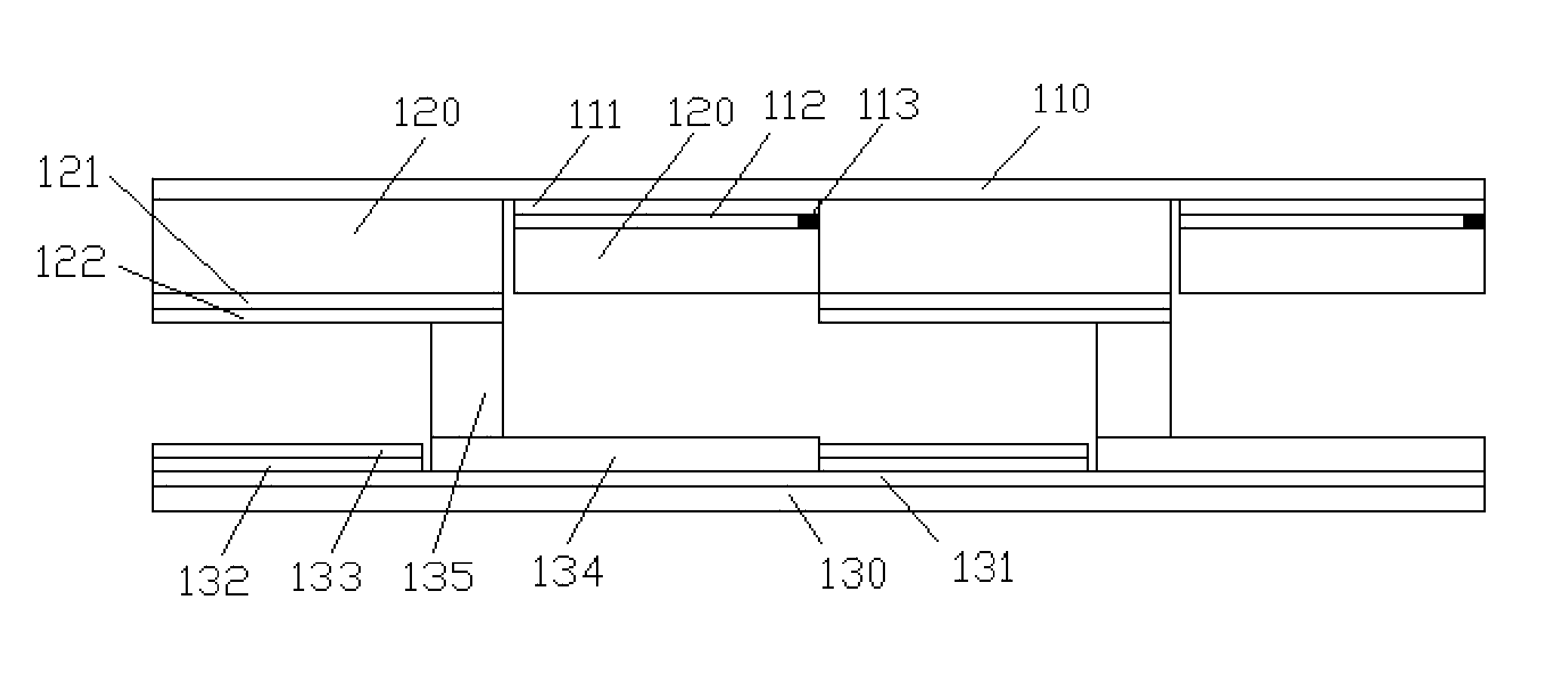
[0023]The triode field emission display with anode and gate on the same substrate presented in the invention, comprising anode-gate substrate and cathode substrate, which are parallel and adapted in the size, wherein: a number of strip-like anode conducting layer are arranged on the anode-gate substrate alternating and side by side, bus electrodes are arranged on the anode conducting layer along the longitudinal centerline, a under-gate dielectric layer is arranged on the anode-gate substrate, the under-gate dielectric layer is composed of a number of longitudinal strips alternating and a number of lateral branch strips arranged on one side or both sides of the longitudinal strips, the longitudinal strips are parallel to anode conducting layer and are arranged on the part of the anode-gate substrate that is not covered by the anode conducting layer, strip-like gate conducting layer and dielectric layer for gate protection are arranged ordinal on the longitudinal strips, the lateral ...


PUM


Abstract

The present invention relates to a triode field emission display with anode and gate on the same substrate, comprising anode-gate substrate and cathode substrate, parallel and adapted in the size; a number of strip-like cathode conducting layers arranged alternating on the cathode substrate; resistor layer for current limiting and dielectric layer for cathode protection are arranged alternately on the cathode conducting layer in the longitudinal direction; the electron emission materials are arranged on the resistor layer for current limiting; wherein the strip-like anode conducting layer and strip-like gate conducting layer on the anode-gate substrate are perpendicular to the strip-like cathode conducting layer on the cathode substrate, dielectric layer for isolation is arranged between the anode-gate and the cathode substrates, one end of the dielectric layer for isolation is connected to the dielectric layer for gate protection, the other end is connected to the dielectric layer for cathode protection.

Description

TECHNICAL FIELD[0001]The present invention relates to the fabrication technique of triode FED and, more particularly, to a novel triode structured filed emission display with anode and gate on the same substrate, and cathode on another substrate.TECHNICAL BACKGROUND OF THE INVENTION[0002]Field emission display (FED) is a novel flat planar display technology, the FED has the advantages of the cathode ray tube (CRT), such as wide viewing angle, colorful, high response speed. Presently, in a variety of flat panel displays, only FED can reach the high image display quality as that of the traditional CRT. The FED also has the advantages of liquid crystal display (LCD), such as thin and slight, as well as small size, light weight, low energy consumption, long life, high image quality. The FED can be classified into diode, triode and multiple structures.[0003]The diode structure FED is composed of anode and cathode, although the fabrication process of diode structure FED is simple, low cos...

Claims


Application Information

Patent Timeline
Patent Type & Authority Patents(United States)
IPC IPC(8): H01J29/32H01J29/08
CPCH01J29/085H01J31/127H01J29/467H01J2329/4634
Inventor GUO, TAILIANGZHANG, YONGAILIN, ZHIXIANHU, LIQINYE, YUNYOU, YUXIANG
Owner GUO TAILIANG
Why Eureka
Try Eureka