
Liquid crystal display device

a liquid crystal display and display device technology, applied in non-linear optics, instruments, optics, etc., can solve the problems of inability to form the above-described slit, the above-described mva mode is not suitable for small pixels, and the transmittance (luminance) greatly deteriorate, so as to achieve stable alignment of liquid crystal molecules, the effect of contrast ratio and viewing angle characteristics

Active Publication Date: 2012-04-03
SHARP KK
View PDF15 Cites 12 Cited by
  • Summary
  • Abstract
  • Description
  • Claims
  • Application Information

AI Technical Summary

Benefits of technology

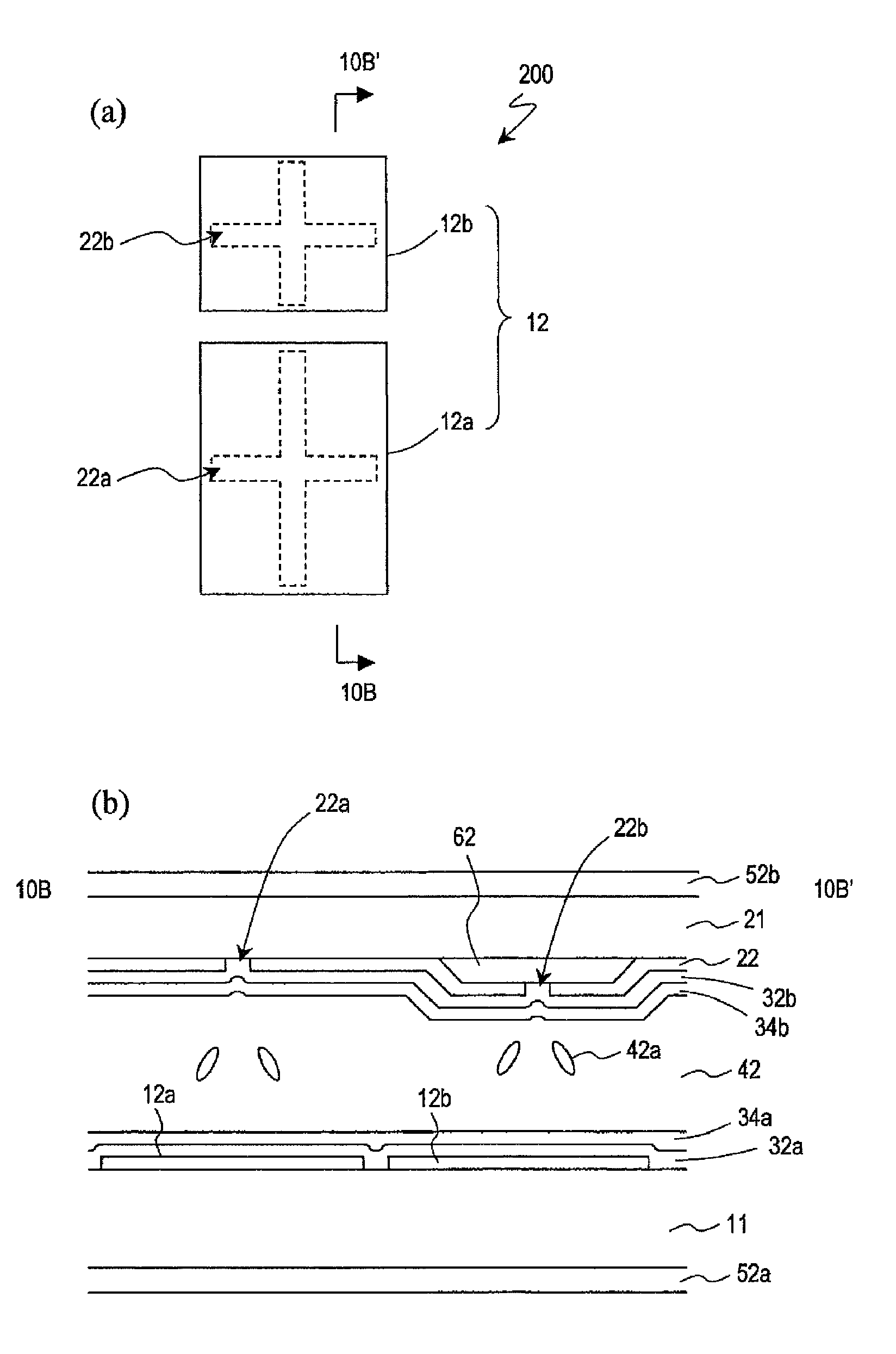
The patent text describes a liquid crystal display device that uses a CPA mode to achieve high transmittance, but also addresses the problem of low contrast ratio and narrow viewing angle. The device includes a pair of polarizing plates and ¼-wave plates to improve the distribution of transmittance in a pixel in a white display state. By omitting the ¼-wave plates, the device achieves high transmittance but decreases in contrast ratio and viewing angle. The text also describes a modification of the device that includes a cruciform slit in the counter electrode to form four domains in the pixel and achieve uniform high transmittance.

Problems solved by technology

However, the above-described MVA mode is not suitable to small pixels (for example, the shorter side is less than 100 μm, specifically less than 60 μm).
If this configuration is applied to a pixel with the shorter side being less than 100 μm, the transmittance (luminance) greatly deteriorates because part of the pixel in which the slits (or ribs) are provided does not contribute to the display.
In such small pixels, even formation of the above-described slit is impossible.
As a matter of course, if the width of the slit is decreased, a sufficient anchoring force cannot be obtained.

Method used


Image

  • Liquid crystal display device
  • Liquid crystal display device
  • Liquid crystal display device

Examples


Embodiment Construction

[0053]Hereinafter, a structure and operation of a liquid crystal display device of an embodiment of the present invention are described with reference to the drawings. Note that the present invention is not limited to the embodiment described below.

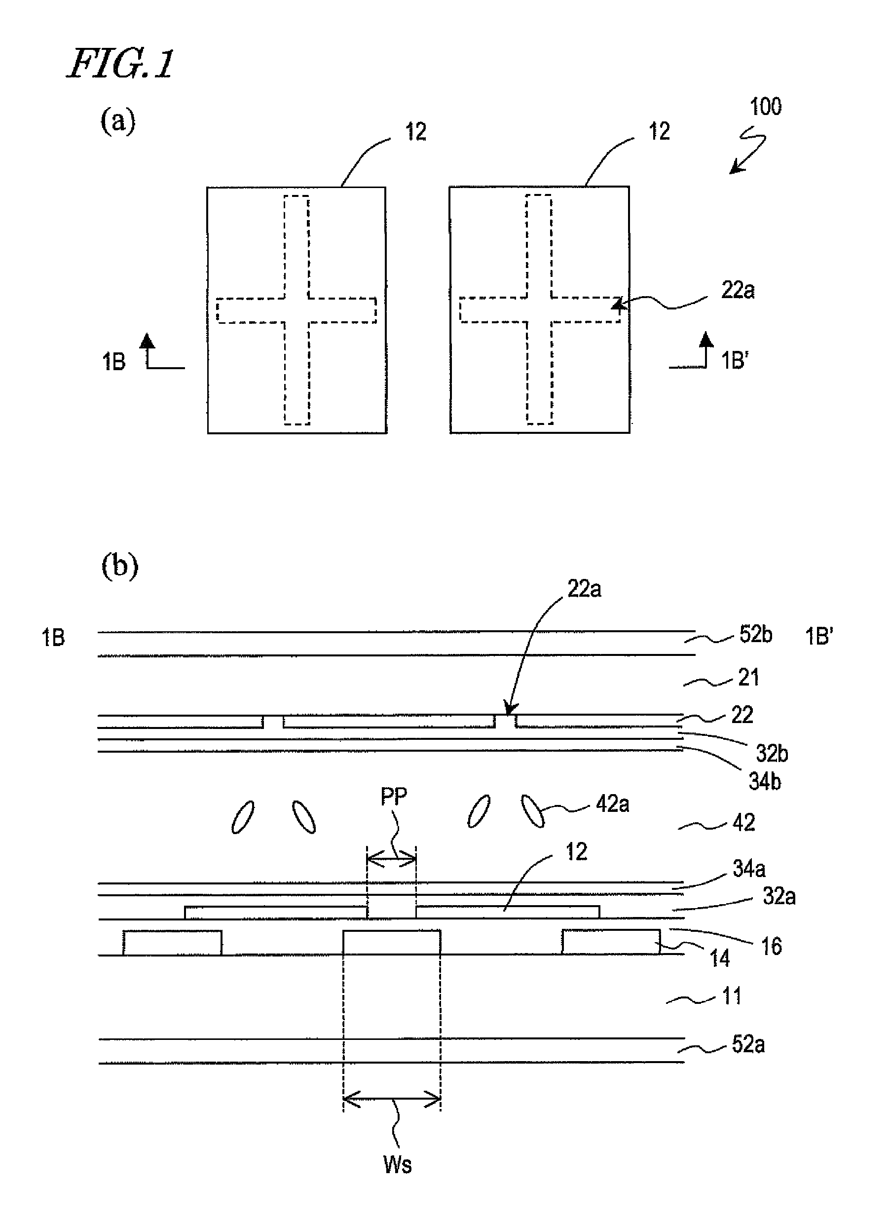
[0054]FIG. 1 schematically shows a structure of two pixels of a liquid crystal display device 100 of an embodiment of the present invention. FIG. 1(a) is a plan view. FIG. 1(b) is a schematic cross-sectional view taken along line 1B-1B′ of FIG. 1(a).

[0055]The liquid crystal display device 100 has a plurality of pixels and includes a pair of substrates 11 and 21 and a pair of polarizing plates 52a and 52b placed in crossed Nicols on the outer sides of the substrates 11 and 21. The liquid crystal display device 100 is configured to display images in a normally black mode. Each pixel has a liquid crystal layer 42 including a nematic liquid crystal material (liquid crystal molecules 42a) whose dielectric anisotropy is negative, and a pixel el...


PUM

PropertyMeasurementUnit
particle diameteraaaaaaaaaa
azimuthal anglesaaaaaaaaaa

Abstract

A VA-mode liquid crystal display device which includes a pair of alignment sustaining layers 34a and 34b formed by a photopolymerized material on surfaces of a pair of vertical alignment films 32a and 32b which are closer to a liquid crystal layer, and a cruciform opening 22a provided only in a counter electrode. When a predetermined voltage is applied across the liquid crystal layer, four liquid crystal domains are formed such that the azimuths of the directors of the respective liquid crystal domains are different from one another and form an angle of about 45′ relative to the polarization axes of a pair of polarizing plates. When no voltage is applied across the liquid crystal layer, the pretilt azimuths of liquid crystal molecules included in regions respectively corresponding to the four liquid crystal domains are regulated by the alignment sustaining layers 34a and 34b.

Description

[0001]This application is the U.S. national phase of International Application No. PCT / JP2008 / 002569, filed 18 Sep. 2008, which designated the U.S. and claims priority to Japanese Patent Application No. 2007-242568, filed 19 Sep. 2007, the entire contents of each of which are hereby incorporated by reference.TECHNICAL FIELD[0002]The present invention relates to a liquid crystal display device and specifically to an alignment control structure preferably applied to a liquid crystal display device which has a relatively small pixel pitch.BACKGROUND ART[0003]Recently, as liquid crystal display devices which have high viewing angle characteristics, transverse electric field mode devices (including IPS mode devices and FES mode devices) and vertical alignment (VA) mode devices are used. The VA mode devices are superior to the transverse electric field mode devices in terms of mass production and therefore have been used in a wide variety of TV applications and mobile applications.[0004]T...

Claims


Application Information

Patent Timeline
Patent Type & Authority Patents(United States)
IPC IPC(8): G02F1/1337
CPCG02F1/133707G02F2001/134318G02F1/134318
Inventor HASHIMOTO, YOSHITOOHGAMI, HIROYUKIKUBO, MASUMISOGA, MASAYUKI
Owner SHARP KK
Learn More