
Techniques of forming Ohmic contacts on GaN light emitting diodes

a technology of gan light emitting diodes and ohmic contacts, which is applied in the direction of basic electric elements, electrical apparatus, and semiconductor devices, can solve the problems of affecting the work function of silver and other materials from which leds are fabricated, and affecting the efficiency of leds

Active Publication Date: 2012-04-03
KORRUS INC
View PDF1 Cites 15 Cited by
  • Summary
  • Abstract
  • Description
  • Claims
  • Application Information

AI Technical Summary

Benefits of technology

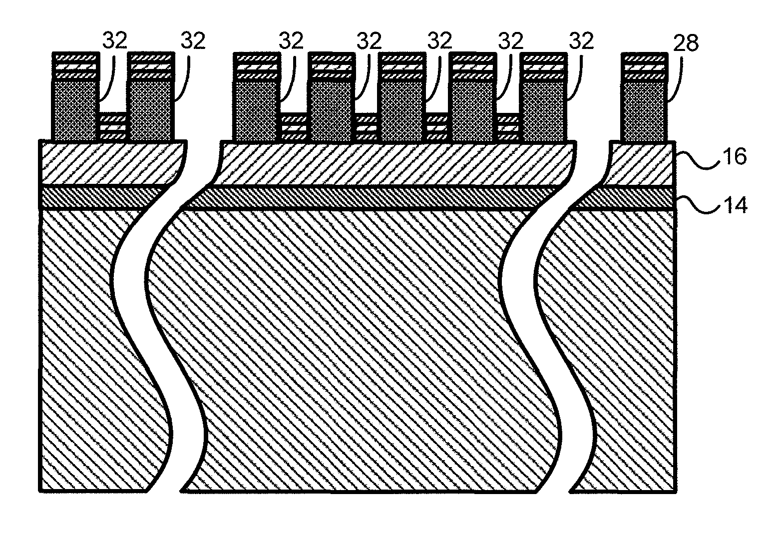
This patent describes a method for making ohmic contacts on a light emitting diode by treating the surface of a layer of p-type gallium nitride with an acid-containing solution and a buffered oxide etch process. This treatment results in a metal stack consisting of layers of silver and platinum on the etched surface. The technical effect of this method is to improve the efficiency and reliability of light emitting diodes by improving the quality of the ohmic contacts.

Problems solved by technology

The difference in the work function between silver and the other materials from which the LED is fabricated has been problematic.
However, surface contamination of the metal semiconductor interface may degrade the ohmic contact performance of metals.
Contamination layers at the interface may produce an unforeseen electronic state that may degrade the efficiency of the LED.

Method used


Image

  • Techniques of forming Ohmic contacts on GaN light emitting diodes
  • Techniques of forming Ohmic contacts on GaN light emitting diodes
  • Techniques of forming Ohmic contacts on GaN light emitting diodes

Examples


Embodiment Construction

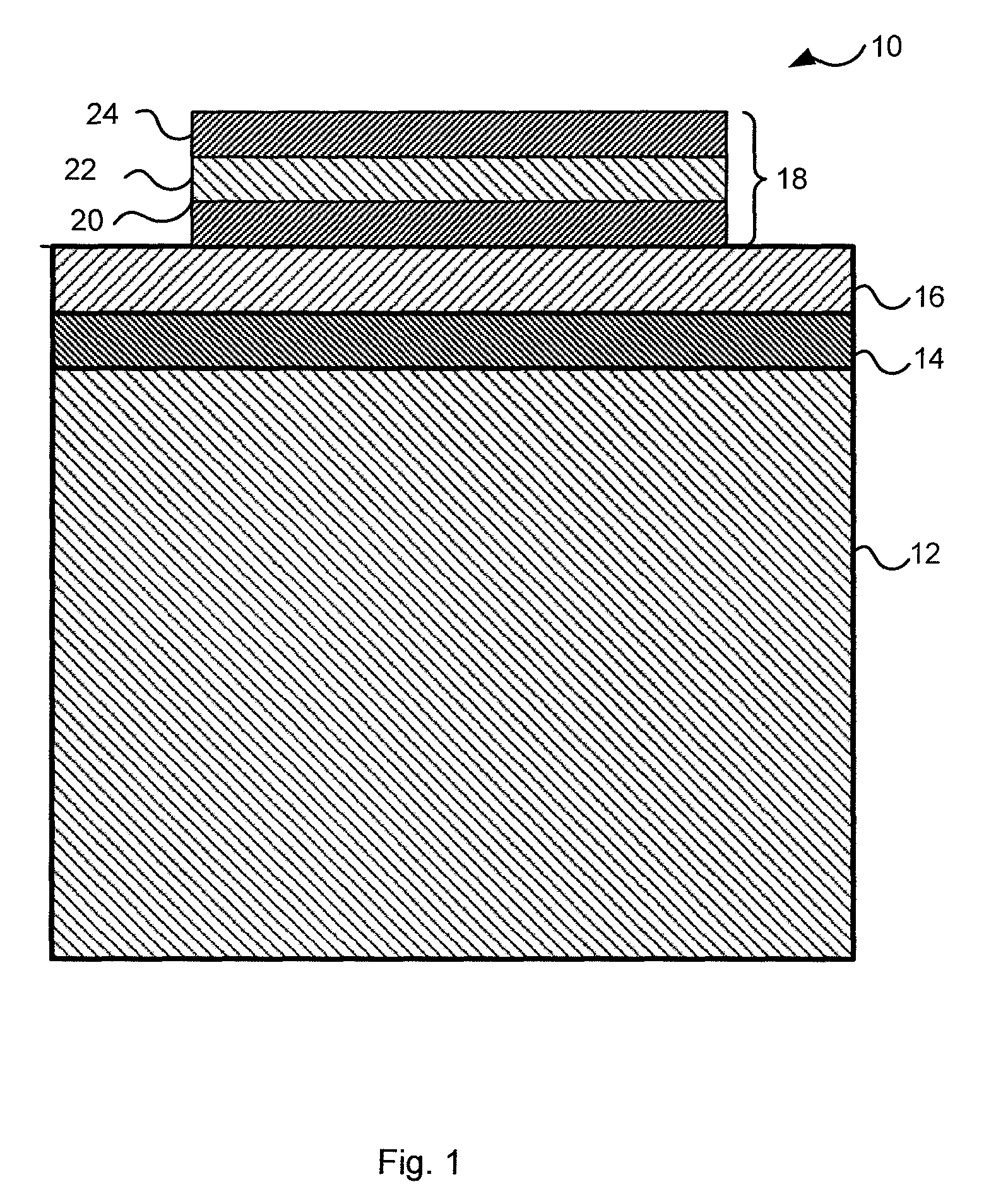
[0014]Referring to FIG. 1, shown is a light emitting diode 10 manufactured in accordance with the present invention that includes a substrate 12 formed of n-type gallium nitride GaN. An active layer 14 is formed upon substrate. Active layer 14 may comprise a single quantum well or multiple quantum wells, with 2-10 quantum wells. A layer of p-type gallium nitride 16 is formed upon quantum wells 14. A metal stack 18 is positioned upon layer 16 and is comprised of three separate metal layers, shown as 20, 22 and 24. Layers 20 and 24 are formed from platinum and layer 22 is formed from silver.

[0015]Substrate 12 may have a large-surface orientation within ten degrees, within five degrees, within two degrees, within one degree, within 0.5 degree, or within 0.2 degree of (0 0 0 1), (0 0 0−1), {1−1 0 0}, {1 1−2 0}, {1−1 0.+−0.1}, {1−1 0.+−0.2}, {1−1 0.+−0.3}, {2 0−2.+−0.1}, or {1 1−2.+−0.2}. In one specific embodiment, the substrate has a semipolar large-surface orientation, which may be de...


PUM

PropertyMeasurementUnit
wavelengthsaaaaaaaaaa
optical absorption coefficientaaaaaaaaaa

Abstract

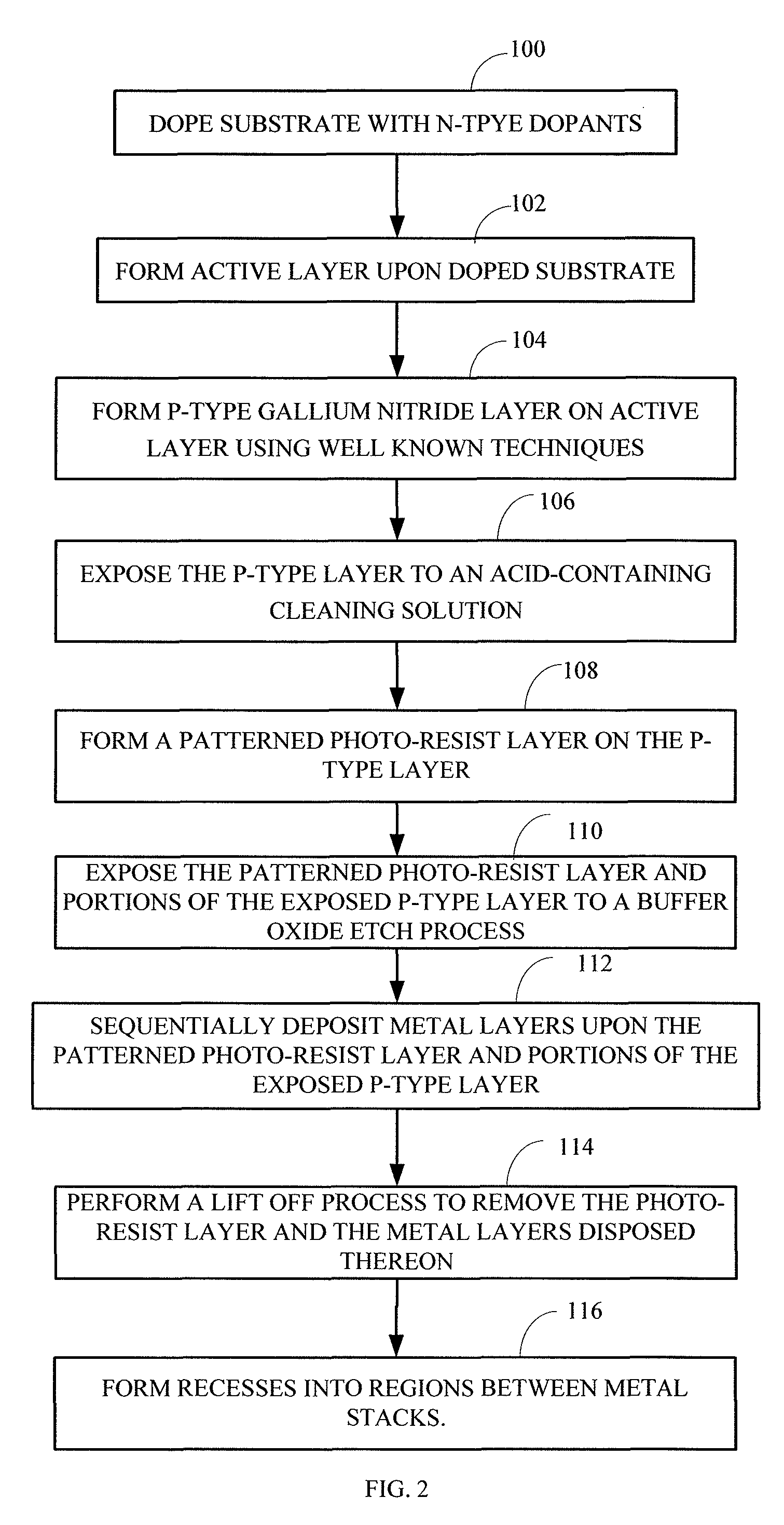
A method of forming ohmic contacts on a light emitting diode that features a surface treatment of a substrate includes exposing a surface of a p-type gallium nitride layer to an acid-containing solution and a buffered oxide etch process. A quantum well is formed in a gallium nitride substrate and a layer of p-type gallium nitride is deposited over the quantum well. The surface of the p-type gallium nitride is exposed to an acid-containing solution and then a buffered oxide etch process is performed to provide an etched surface. A metal stack including a layer of silver disposed between layers of platinum is then deposited.

Description

BACKGROUND OF THE INVENTION[0001]The invention is directed to light emitting diodes and in particular to ohmic contacts for light emitting diodes.[0002]One technique for measuring the efficiency of light emitting diodes (LEDs) is by determining the luminance per watt. The luminance provided by light emitting diodes is dependent upon several factors such as internal quantum efficiencies, as in the case of an injected carrier not being converted to a photon, or extraction efficiency, as in the case of a small fraction of photons being successfully extracted from the light emitting diode as opposed to being lost to internal absorption. To realize high efficiency LEDS, both of these issues need to be addressed. The potential gain from improving extraction efficiency, however, is likely to be greater and simpler to accomplish than the gains from improving internal efficiency.[0003]One technique to improve light extraction of visible light nitride LEDs, such as Gallium Nitride (GaN) LEDs,...

Claims


Application Information

Patent Timeline
Patent Type & Authority Patents(United States)
IPC IPC(8): H01L21/00
CPCH01L33/0075H01L33/405H01L2933/0016
Inventor FELKER, ANDREW J.VICKERS, NICHOLAS ANDREW
Owner KORRUS INC
Learn More