P+ polysilicon material on aluminum for non-volatile memory device and method

a memory device and polysilicon technology, applied in semiconductor devices, semiconductor/solid-state device details, electrical devices, etc., can solve problems such as non-scaling of sub-threshold slopes, increase power dissipation, and degrade device performan

Active Publication Date: 2012-01-03
CROSSBAR INC
View PDF1 Cites 98 Cited by
  • Summary
  • Abstract
  • Description
  • Claims
  • Application Information

AI Technical Summary

Problems solved by technology

However, as field effect transistors (FET) approach sizes less than 100 nm, problems such as short channel effect can degrade device performance.
Moreover, such sub 100 nm device size can lead to sub-threshold slope non-scaling and also increases power dissipation.
These devices often require new materials and device structures to couple with silicon-based devices to form a memory cell, which lack one or more key attributes.
For example, Fe-RAM and MRAM devices have fast switching characteristics and good programming endurance, but their fabrication is not CMOS compatible and size is usually large.
Switching for a PCRAM device requires large amounts of power.
Organic RAM or ORAM is incompatible with large volume silicon-based fabrication and device reliability is usually poor.

Method used


Image

  • P+ polysilicon material on aluminum for non-volatile memory device and method
  • P+ polysilicon material on aluminum for non-volatile memory device and method
  • P+ polysilicon material on aluminum for non-volatile memory device and method

Examples


Embodiment Construction

[0013]The present invention is directed to switching devices. More particularly, embodiments according to the present invention provide a method and a device structure for a resistive switching device. The resistive switching device can be used as a non-volatile memory device but it should be recognized that the present invention can have a much broader range of applicability

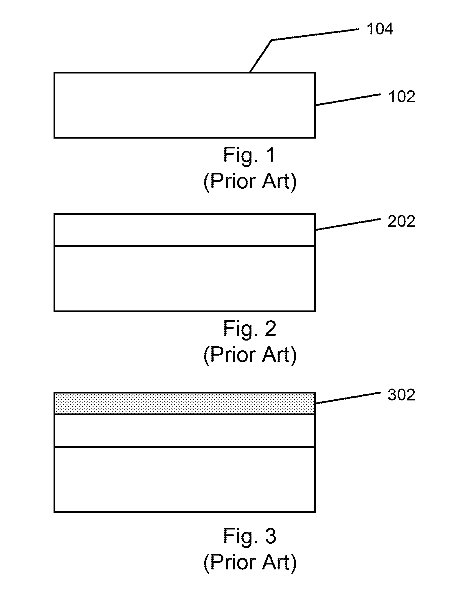
[0014]FIGS. 1-5 illustrate part of the steps of a conventional method for forming a non volatile memory device. As shown, the conventional method includes provided a semiconductor substrate 102 having a surface region 104. The semiconductor substrate can be single crystal silicon, silicon on insulator, silicon germanium or other suitable material. A first dielectric material 202 is formed overlying a surface region of the semiconductor substrate. The first dielectric material can be silicon oxide or silicon nitride or a low K dielectric, or a high K dielectric or a dielectric stack depending on the application. ...


PUM

PropertyMeasurementUnit
sizesaaaaaaaaaa
sizeaaaaaaaaaa
thicknessaaaaaaaaaa

Abstract

A method of forming a non-volatile memory device. The method includes providing a substrate having a surface region and forming a first dielectric material overlying the surface region. A first wiring material comprising at least an aluminum material is formed overlying the first dielectric material. The method forms a silicon material overlying the aluminum material and forms an intermix region consuming a portion of the silicon material and a portion of the aluminum material. The method includes an annealing process to cause formation of a first alloy material from the intermix region and a polycrystalline silicon material having a p+ impurity characteristic overlying the first alloy material. A first wiring structure is formed from at least a portion of the first wiring material. A resistive switching element comprising an amorphous silicon material is formed overlying the polycrystalline silicon material having the p+ impurity characteristic. A second wiring structure comprising at least a metal material is formed overlying the resistive switching element.

Description

CROSS REFERENCE TO RELATED APPLICATIONS[0001]Not ApplicableSTATEMENT RELATED TO FEDERAL OR GOVERNMENT SPONSORED RESEARCH[0002]Not ApplicableBACKGROUND[0003]The present invention is directed to switching devices. More particularly, embodiments according to the present invention provide a method and a device structure for a resistive switching device. The resistive switching device can be used as a non-volatile memory device but it should be recognized that the present invention can have a much broader range of applicability.[0004]The success of semiconductor devices has been mainly driven by an intensive transistor down-scaling process. However, as field effect transistors (FET) approach sizes less than 100 nm, problems such as short channel effect can degrade device performance. Moreover, such sub 100 nm device size can lead to sub-threshold slope non-scaling and also increases power dissipation. It is generally believed that transistor-based memories such as those commonly known as...

Claims


Application Information

Patent Timeline
Patent Type & Authority Patents(United States)
IPC IPC(8): H01L21/44H01L29/02H01L29/40
CPCH01L27/2409H01L27/2463H01L45/085H01L45/1233H01L45/148H01L45/1683H10B63/80H10N70/245H10N70/841H10N70/884H10N70/011H10N70/826H10N70/066
Inventor HERNER, SCOTT BRAD
Owner CROSSBAR INC
Why Eureka
Try Eureka