
Package structure and manufacturing method thereof

a technology of packaging and manufacturing method, applied in the direction of semiconductor devices, semiconductor/solid-state device details, electrical devices, etc., can solve the problems of reducing the distance of the signal transmission path, affecting the operability, performance and life of the ic chip, and the traditional package technique cannot meet the demand of producing a smaller chip with high density elements on the chip, etc., to achieve the effect of reducing the thickness of the package structur

Active Publication Date: 2011-11-15
SAMSUNG ELECTRONICS CO LTD
View PDF2 Cites 5 Cited by
  • Summary
  • Abstract
  • Description
  • Claims
  • Application Information

AI Technical Summary

Benefits of technology

[0012]In view of foregoing, the present invention provides a semiconductor device package structure, which is utilized by redistribution layer (RDL) and through silicon via (TSV) techniques and minimizes the thickness of package structure for a wafer level chip scale package.
[0013]An object of the present invention is to provide a structure for chip scale package, which can allow minimizing the size of chip scale package.
[0014]A further object of the present invention is to provide a structure for producing smaller chip with high pin count or high density elements on the chip, high performance and high reliability package.
[0015]Another object of the present invention is to provide a convenient, cost-effective method for manufacturing a semiconductor device package.

Problems solved by technology

As a semiconductor becomes more complicated, the traditional package technique, for example lead frame package, flex package, and rigid package techniques, cannot meet the demand of producing a smaller chip with high density elements on the chip.
Further, the operability, performance, and life of an IC chip are greatly affected by its circuit design, wafer manufacturing, and chip packaging.
As a result, this method fails to reduce the distance of the signal transmission path but in fact increase the signal path distance.
This will increase signal delay and attenuation and decrease the performance of the chip.
Although WLCSP can greatly reduce the signal path distance, it is still very difficult to accommodate all the bonding points on the die surface as the integration of die and internal components gets higher.
The pin count on the die increases as integration gets higher so the redistribution of pins in an area array is difficult to achieve.
Even if the redistribution of pins is successful, the distance between pins will suffer yield and reliability issues owing to the huge size of the package.
The further disadvantages of the former method are higher costs and time-consuming for manufacture.

Method used


Image

  • Package structure and manufacturing method thereof
  • Package structure and manufacturing method thereof
  • Package structure and manufacturing method thereof

Examples


first embodiment

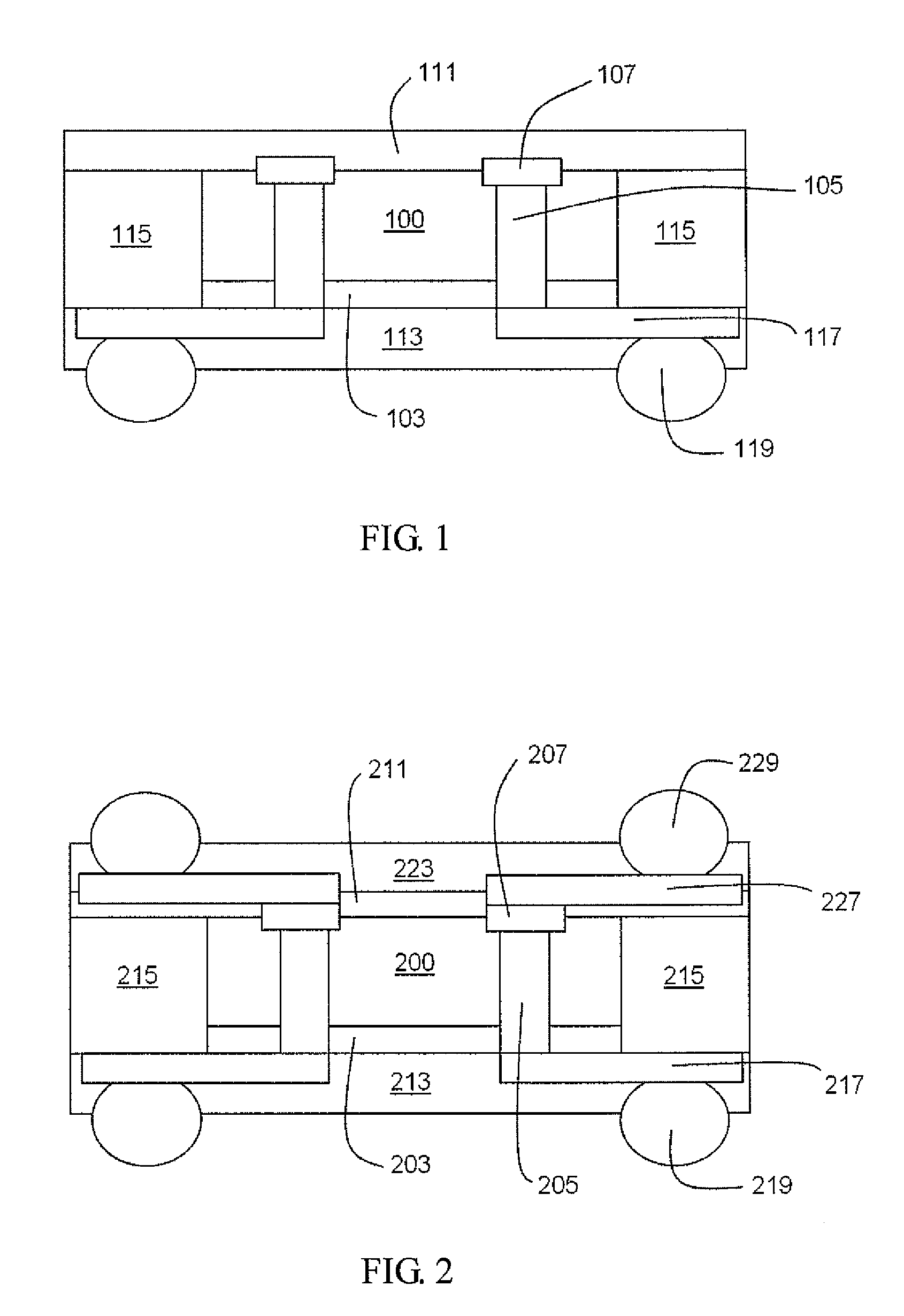
[0029]FIG. 1 illustrates a cross-sectional view of a semiconductor device package structure according to the present invention. As shown in FIG. 1, a semiconductor device package structure includes an electronic element 100, which comprises an active surface and a backside surface, and includes a dielectric (isolation) layer 103 formed on the backside surface of the electronic element 100. A plurality of conductive through vias 105 cross through the electronic element 100 and the dielectric layer 103, and a plurality of conductive pads 107 accompany the conductive through vias 105 disposed on the active surface of the electronic element 100. A filler 115 is adjacent to the side wall of the electronic element 100 and the side wall of the dielectric layer 103. A redistribution layer 117 is formed under the dielectric layer 103 and connects to the conductive through vias 105. A first protective layer 111 is formed to cover and protect the active surface of electronic element 100, the c...

second embodiment

[0034]FIG. 2 illustrates a cross-section view of a stacked semiconductor device package structure according to the present invention. As shown in FIG. 2, a stacked semiconductor device package structure includes electronic element 200, which comprises an active surface and a backside surface and includes a dielectric (isolation) layer 203 formed on the backside surface of the electronic element 200. A plurality of conductive through vias 205 cross through the electronic element 200 and the dielectric layer 203, and a plurality of conductive pads 207 accompany the conductive through vias 205 disposed on the active surface of the electronic element 200. A filler 215 is adjacent to the side wall of the electronic element 200 and the side wall of the dielectric layer 203. A first redistribution layer 217 is formed under the dielectric layer 203 and connects to the conductive through vias 205. A first protective layer 211 is formed to cover and protect the active surface of electronic el...

third embodiment

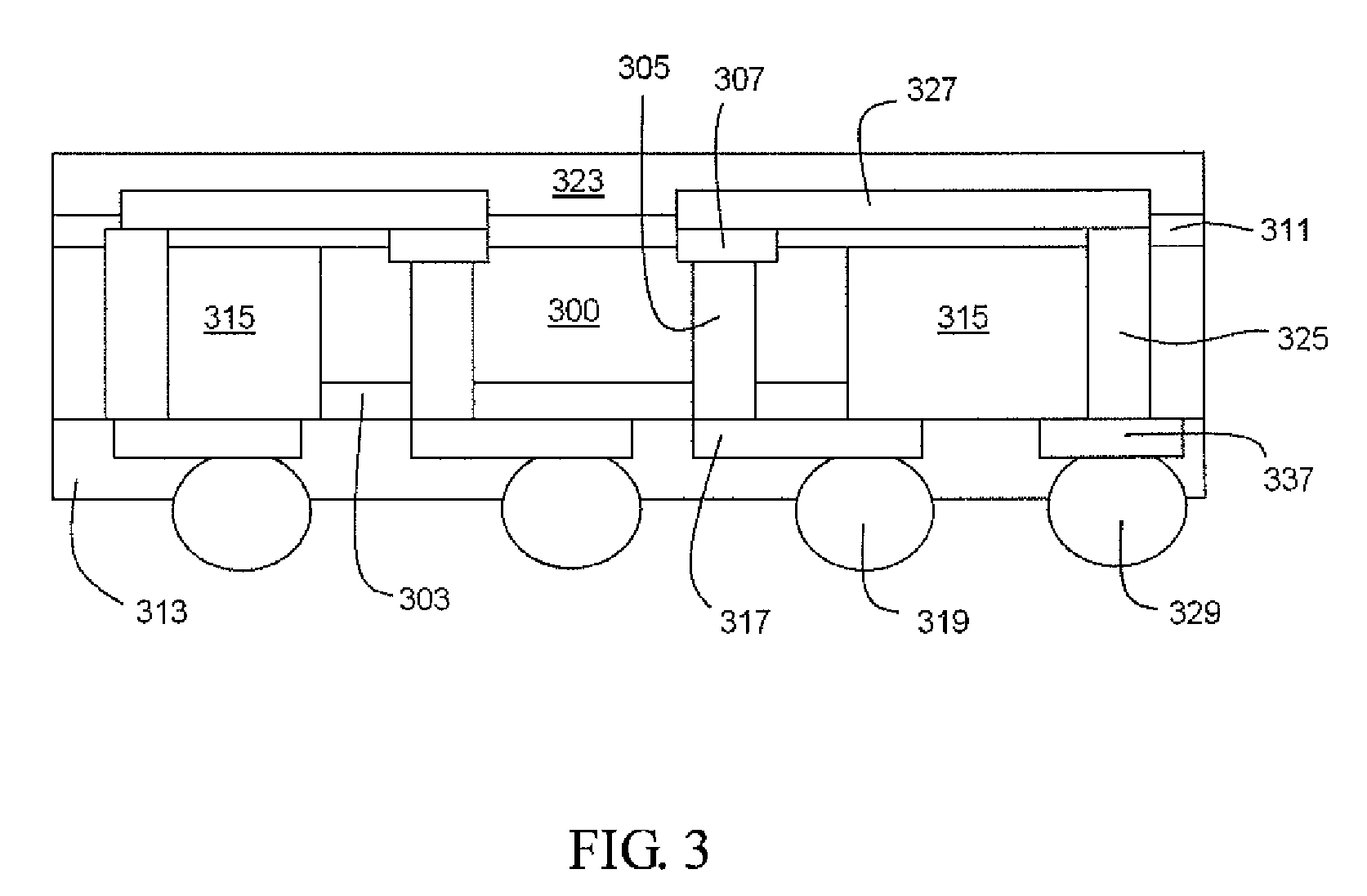
[0039]FIG. 3 illustrates a cross-section view of a semiconductor device package structure according to the present invention. As shown in FIG. 3, a semiconductor device package structure includes an electronic element 300, which comprises an active surface and a backside surface and includes a dielectric (isolation) layer 303 formed on the backside surface of the electronic element 300. A plurality of first conductive through vias 305 cross through the electronic element 300 and the dielectric layer 303, and a plurality of conductive pads 307 accompany the first conductive through vias 305 disposed on the active surface of the electronic element 300. A filler 315 is adjacent to the side wall of the electronic element 300 and the side wall of the dielectric layer 303. A first redistribution layer 317 is formed under the dielectric layer 303 and connects to the conductive through vias 305. A plurality of second conductive through vias 325 further formed across through the filler 315. ...


PUM


Abstract

The present invention discloses a semiconductor device package structure with redistribution layer (RDL) and through silicon via (TSV) techniques. The package structure comprises an electronic element which includes a dielectric layer on a backside surface of the electronic element, a plurality of first conductive through vias across through the electronic element and the dielectric layer, and a plurality of conductive pads accompanying the first conductive through vias on an active surface of the electronic element; a filler material disposed adjacent to the electronic element; a first redistribution layer disposed over the dielectric layer and the filler material, and connected to the first conductive through vias; a first protective layer disposed over the active surface of the electronic element, the conductive pads, and the filler material; and a second protective layer disposed over the redistribution layer, the dielectric layer, and the filler material.

Description

FIELD OF THE INVENTION[0001]This invention relates to a structure of a package, and more particularly to a semiconductor device package structure with redistribution layers (RDL) and through silicon via (TSV) techniques.BACKGROUND OF THE INVENTION[0002]In recent years, the high-technology electronics manufacturing industries launch more feature-packed and humanized electronic products. These new products that hit the showroom are lighter, thinner, and smaller in design. In the manufacturing of these electronic products, the key component has to be the integrated circuit (IC) chip inside any electronic product.[0003]Rapid development of semiconductor technology has led to rapid progress of a reduction in size of semiconductor packages, the adoption of multi-pin, the adoption of fine pitch, the minimization of electronic components and the like. The purposes and the advantages of wafer level package includes decreasing the production cost, decreasing the effect caused by the parasitic...

Claims


Application Information

Patent Timeline
Patent Type & Authority Patents(United States)
IPC IPC(8): H01L21/48
CPCH01L23/3107H01L23/481H01L23/3185H01L23/49816H01L24/05H01L24/13H01L2924/30107H01L2224/20H01L2924/01078H01L2924/01079H01L2924/14H01L2924/15311H01L2224/04105H01L2224/0401H01L24/19H01L2224/12105H01L2224/2518
Inventor LIN, DIANN-FANGHU, YU-SHAN
Owner SAMSUNG ELECTRONICS CO LTD
Learn More